MPC7447A Ver la hoja de datos (PDF) - Freescale Semiconductor
Número de pieza
componentes Descripción
Fabricante
MPC7447A Datasheet PDF : 56 Pages
| |||
Electrical and Thermal Characteristics
5.2.3 IEEE 1149.1 AC Timing Specifications
Table 10 provides the IEEE 1149.1 (JTAG) AC timing specifications as defined in Figure 16 through
Figure 19.
Table 10. JTAG AC Timing Specifications (Independent of SYSCLK)1
At recommended operating conditions. See Table 4.
Parameter
Symbol
Min
Max
Unit Notes
TCK frequency of operation
fTCLK
0
33.3
MHz
TCK cycle time
tTCLK
30
—
ns
TCK clock pulse width measured at 1.4 V
tJHJL
15
—
ns
TCK rise and fall times
tJR and tJF
—
2
ns
TRST assert time
tTRST
25
—
ns
2
Input setup times:
Boundary-scan data
TMS, TDI
tDVJH
4
tIVJH
0
ns
3
—
—
Input hold times:
Boundary-scan data
TMS, TDI
tDXJH
20
tIXJH
25
ns
3
—
—
Valid times:
Boundary-scan data
TDO
ns
4
tJLDV
4
20
tJLOV
4
25
Output hold times:
Boundary-scan data
TDO
tJLDX
30
tJLOX
30
ns
4
—
—
TCK to output high impedance:
Boundary-scan data
TDO
ns
4, 5
tJLDZ
3
19
tJLOZ
3
9
Notes:
1. All outputs are measured from the midpoint voltage of the falling/rising edge of TCLK to the midpoint of the signal
in question. The output timings are measured at the pins. All output timings assume a purely resistive 50-Ω load
(see Figure 7). Time-of-flight delays must be added for trace lengths, vias, and connectors in the system.
2. TRST is an asynchronous level sensitive signal. The time is for test purposes only.
3. Non-JTAG signal input timing with respect to TCK.
4. Non-JTAG signal output timing with respect to TCK.
5. Guaranteed by design and characterization.
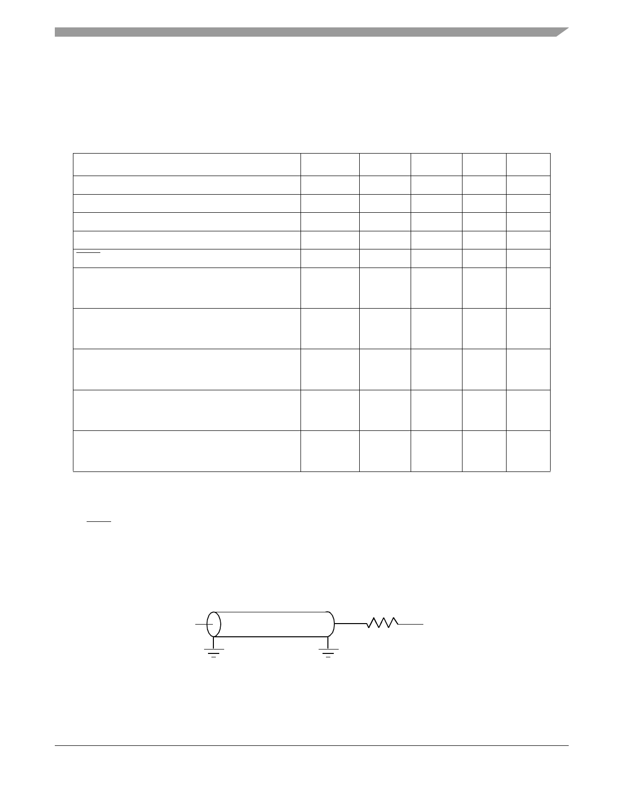
Figure 7 provides the AC test load for TDO and the boundary-scan outputs of the MPC7447A.
Output
Z0 = 50 Ω
RL = 50 Ω
OVDD/2
Figure 7. Alternate AC Test Load for the JTAG Interface
MPC7447A RISC Microprocessor Hardware Specifications, Rev. 5
Freescale Semiconductor
19
Share Link: 