TE28F400B3T110 Ver la hoja de datos (PDF) - Intel
Número de pieza
componentes Descripción
Fabricante
TE28F400B3T110 Datasheet PDF : 48 Pages
| |||
E
SMART 3 ADVANCED BOOT BLOCK
Symbol
VCCQ
VCC
VPP
GND
NC
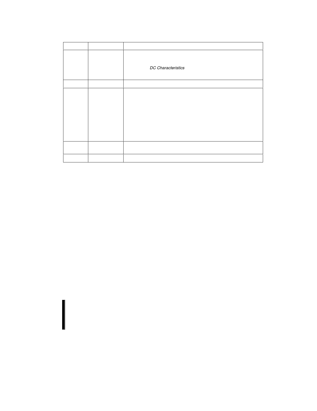
Table 2. Smart 3 Advanced Boot Block Pin Descriptions (Continued)
Type
Name and Function
INPUT
OUTPUT VCC: Enables all outputs to be driven to 1.8 V – 2.5 V while
the VCC is at 2.7 V–3.3 V. If the VCC is regulated to 2.7 V–2.85 V, VCCQ
can be driven at 1.65 V–2.5 V to achieve lowest power operation (see
Section 4.4, DC Characteristics.
This input may be tied directly to VCC (2.7 V–3.6 V).
DEVICE POWER SUPPLY: 2.7 V–3.6 V
PROGRAM/ERASE POWER SUPPLY: Supplies power for program
and erase operations. VPP may be the same as VCC (2.7 V–3.6 V) for
single supply voltage operation. For fast programming at manufacturing,
11.4 V–12.6 V may be supplied to VPP. This pin cannot be left floating.
Applying 11.4 V–12.6 V to VPP can only be done for a maximum of 1000
cycles on the main blocks and 2500 cycles on the parameter blocks.
VPP may be connected to 12 V for a total of 80 hours maximum (see
Section 3.4 for details).
VPP < VPPLK protects memory contents against inadvertent or
unintended program and erase commands.
GROUND: For all internal circuitry. All ground inputs must be
connected.
NO CONNECT: Pin may be driven or left floating.
2.2 Block Organization
The Smart 3 Advanced Boot Block is an
asymmetrically-blocked architecture that enables
system integration of code and data within a single
flash device. Each block can be erased
independently of the others up to 100,000 times.
For the address locations of each block, see the
memory maps in Appendix D.
2.2.1
PARAMETER BLOCKS
The Smart 3 Advanced Boot Block flash memory
architecture includes parameter blocks to facilitate
storage of frequently updated small parameters
(e.g., data that would normally be stored in an
EEPROM). By using software techniques, the word-
rewrite functionality of EEPROMs can be emulated.
Each device contains eight parameter blocks of
8-Kbytes/4-Kwords (8192 bytes/4,096 words) each.
2.2.2
MAIN BLOCKS
After the parameter blocks, the remainder of the
array is divided into equal size main blocks (65,536
bytes / 32,768 words) for data or code storage. The
4-Mbit device contains seven main blocks; 8-Mbit
device contains fifteen main blocks; 16-Mbit flash
has thirty-one main blocks; 32-Mbit has sixty-three
main blocks.
3.0 PRINCIPLES OF OPERATION
Flash memory combines EEPROM functionality
with in-circuit electrical program and erase
capability. The Smart 3 Advanced Boot Block flash
memory family utilizes a Command User Interface
(CUI) and automated algorithms to simplify program
and erase operations. The CUI allows for 100%
CMOS-level control inputs and fixed power supplies
during erasure and programming.
PRELIMINARY
11
Share Link: 