ICL7109 Ver la hoja de datos (PDF) - Intersil
Número de pieza
componentes Descripción
Fabricante
ICL7109 Datasheet PDF : 25 Pages
| |||
ICL7109
Reference Voltage
The analog input required to generate a full scale output of
4096 counts is VIN = 2VREF . For normalized scale, a refer-
ence of 2.048V should be used for a 4.096V full scale, and
204.8mV should be used for a 0.4096V full scale. However,
in many applications where the A/D is sensing the output of
a transducer, there will exist a scale factor other than unity
between the absolute output voltage to be measured and a
desired digital output. For instance, in a weighing system,
the designer might like to have a full scale reading when the
voltage from the transducer is 0.682V. Instead of driving the
input down to 409.6mV, the input voltage should be mea-
sured directly and a reference voltage of 0.341V should be
used. Suitable values for integrating resistor and capacitor
are 33kΩ and 0.15µF. This avoids a divider on the input.
Another advantage of this system occurs when a zero read-
ing is desired for non-zero input. Temperature and weight
measurements with an offset or tare are examples. The off-
set may be introduced by connecting the voltage output of
the transducer between common and analog high, and the
offset voltage between common and analog low, observing
polarities carefully. However, in processor-based systems
using the ICL7109, it may be more efficient to perform this
type of scaling or tare subtraction digitally using software.
Reference Sources
The stability of the reference voltage is a major factor in the
overall absolute accuracy of the converter. The resolution of
the ICL7109 at 12 bits is one part in 4096, or 244ppm. Thus
if the reference has a temperature coefficient of 80ppm/oC
(onboard reference) a temperature difference of 3oC will
introduce a one-bit absolute error.
For this reason, it is recommended that an external high-
quality reference be used where the ambient temperature is
not controlled or where high-accuracy absolute measure-
ments are being made.
The ICL7109 provides a REFerence OUTput (Pin 29) which
may be used with a resistive divider to generate a suitable
reference voltage. This output will sink up to about 20mA
without significant variation in output voltage, and is provided
with a pullup bias device which sources about 10µA. The
output voltage is nominally 2.8V below V+, and has a tem-
perature coefficient of ±80ppm/oC (Typ). When using the
onboard reference, REF OUT (Pin 29) should be connected
to REF- (Pin 39), and REF+ should be connected to the
wiper of a precision potentiometer between REF OUT and
V+. The circuit for a 204.8mV reference is shown in the test
circuit. For a 2.048mV reference, the fixed resistor should be
removed, and a 25kΩ precision potentiometer between REF
OUT and V+ should be used.
Note that if Pins 29 and 39 are tied together and Pins 39 and
40 accidentally shorted (e.g., during testing), the reference
supply will sink enough current to destroy the device. This can
be avoided by placing a 1kΩ resistor in series with Pin 39.
Detailed Description
Digital Section
The digital section includes the clock oscillator and scaling
circuit, a 12-bit binary counter with output latches and TTL-
compatible three-state output drivers, polarity, over-range
and control logic, and UART handshake logic, as shown in
Figure 4.
Throughout this description, logic levels will be referred to as
“low” or “high”. The actual logic levels are defined in the Elec-
trical Specifications Table. For minimum power consumption,
all inputs should swing from GND (low) to V+ (high). Inputs
driven from TTL gates should have 3-5kΩ pullup resistors
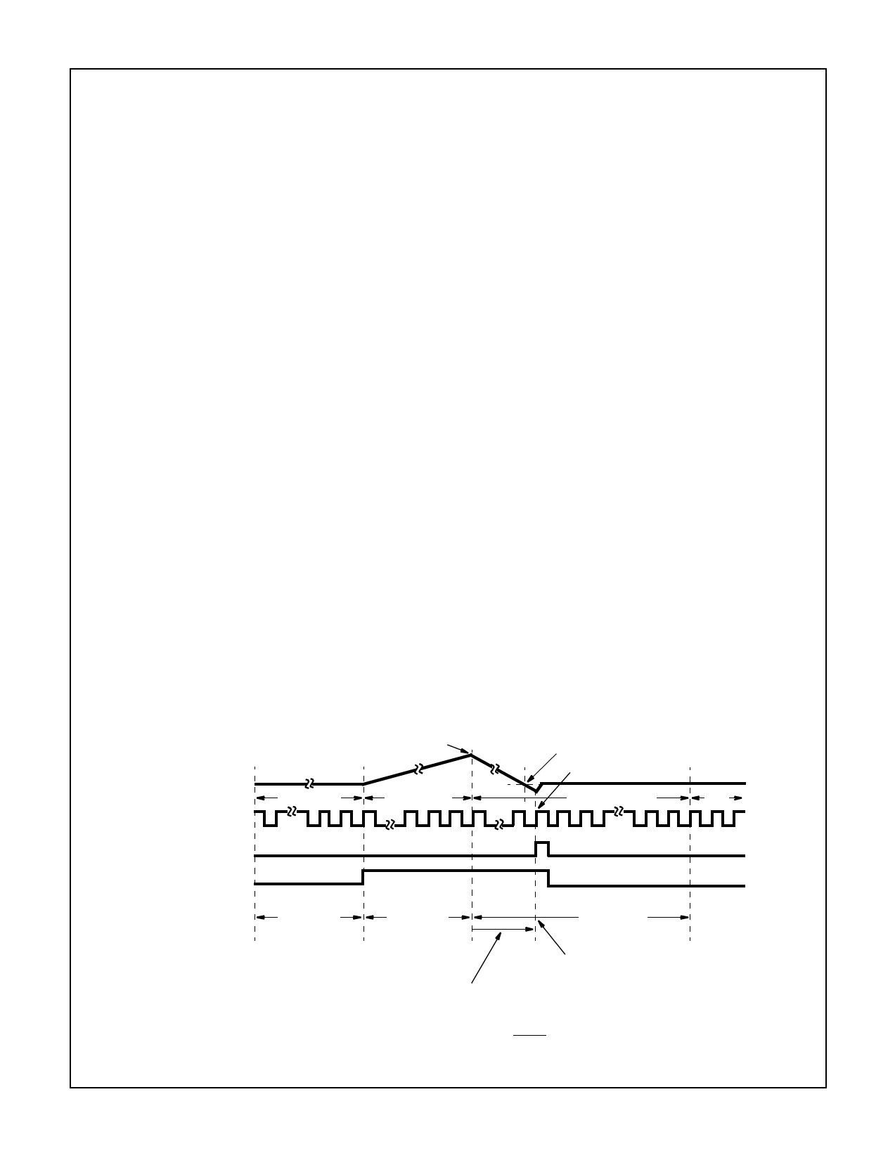
INTEGRATOR
OUTPUT
INTERNAL CLOCK
AZ PHASE I
INTERNAL LATCH
STATUS OUTPUT
2048 COUNTS
MINIMUM
POLARITY
DETECTED
INT PHASE II
FIXED 2048
COUNTS
NUMBER OF COUNTS TO ZERO CROSSING
PROPORTIONAL TO VIN
ZERO CROSSING
OCCURS
ZERO CROSSING
DETECTED
DEINT PHASE III
AZ
4096 COUNTS
MAX
AFTER ZERO CROSSING
ANALOG SECTION WILL
BE IN AUTOZERO
CONFIGURATION
MODE Input
FIGURE 3. CONVERSION TIMING (RUN/HOLD PIN HIGH)
The MODE input is used to control the output mode of the
11
Share Link: 