ICL7109 Ver la hoja de datos (PDF) - Intersil
Número de pieza
componentes Descripción
Fabricante
ICL7109 Datasheet PDF : 25 Pages
| |||
ICL7109
INTEGRATOR
OUTPUT
ZERO CROSSING
OCCURS ZERO CROSSING
DETECTED
INTERNAL
CLOCK
INTERNAL
LATCH
STATUS
OUTPUT
MODE
INPUT
MODE HIGH ACTIVATES
INTERNAL
UART
NORM
CE/LOAD,
HBEN,
LBEN
MODE
SEND
INPUT
SEND
SENSED
CE/LOAD
HBEN
HIGH BYTE
DATA
LBEN
DATA VALID
SEND
SENSED
TERMINATES
UART MODE
MODE LOW, NOT
IN HANDSHAKE MODE
DISABLES OUTPUTS CE/LOAD, HBEN, LBEN
LOW BYTE
DATA
DATA VALID
= DON’T CARE
= THREE-STATE HIGH IMPEDANCE
= THREE-STATE WITH PULLUP
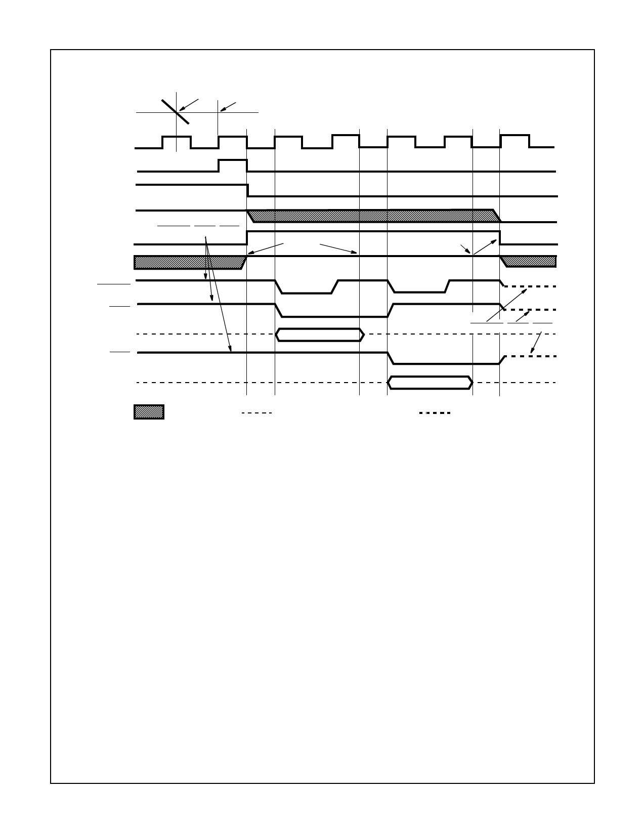
FIGURE 7. HANDSHAKE WITH SEND HELD HIGH
Assuming the UART Transmitter Buffer Register is empty, the
SEND input will be high when the handshake mode is entered
after new data is stored. The CE/LOAD and HBEN terminals will
go low after SEND is sensed, and the high order byte outputs
become active. When CE/LOAD goes high at the end of one
clock period, the high order byte data is clocked into the UART
Transmitter Buffer Register. The UART TBRE output will now go
low, which halts the output cycle with the HBEN output low, and
the high order byte outputs active. When the UART has trans-
ferred that data to the Transmitter Register and cleared the
Transmitter Buffer Register, the TBRE returns high. On the next
ICL7109 internal clock high to low edge, the high order byte out-
puts are disabled, and one-half internal clock later, the HBEN
output returns high. At the same time, the CE/LOAD and LBEN
outputs go low, and the low order byte outputs become active.
Similarly, when the CE/LOAD returns high at the end of one
clock period, the low order data is clocked into the UART Trans-
mitter Buffer Register, and TBRE again goes low. When TBRE
returns to a high it will be sensed on the next ICL7109 internal
clock high to low edge, disabling the data outputs. One-half
internal clock later, the handshake mode will be cleared, and the
CE/LOAD, HBEN and LBEN terminals return high and stay
inactive (as long as MODE stays high).
With the MODE input remaining high as in these examples,
the converter will output the results of every conversion
except those completed during a handshake operation. By
triggering the converter into handshake mode with a low to
high edge on the MODE input, handshake output
sequences may be performed on demand. Figure 9 shows
a handshake output sequence triggered by such an edge.
In addition, the SEND input is shown as being low when the
converter enters handshake mode. In this case, the whole
output sequence for the first (high order) byte is similar to
the sequence for the second byte. This diagram also shows
the output sequence taking longer than a conversion cycle.
Note that the converter still makes conversions, with the
STATUS output and RUN/HOLD input functioning nor-
mally. The only difference is that new data will not be
latched when in handshake mode, and is therefore lost.
Oscillator
The ICL7109 is provided with a versatile three terminal
oscillator to generate the internal clock. The oscillator may be
overdriven, or may be operated with an RC network or crystal.
The OSCILLATOR SELECT input changes the internal config-
uration of the oscillator to optimize it for RC or crystal operation.
When the OSCILLATOR SELECT input is high or left open
(the input is provided with a pullup resistor), the oscillator is
configured for RC operation, and the internal clock will be of
the same frequency and phase as the signal at the
BUFFERED OSCILLATOR OUTPUT. The resistor and
capacitor should be connected as in Figure 10. The circuit will
oscillate at a frequency given by f = 0.45/RC. A 100kΩ resistor
is recommended for useful ranges of frequency. For optimum
60Hz line rejection, the capacitor value should be chosen
15
Share Link: 