ICL7109 Ver la hoja de datos (PDF) - Intersil
Número de pieza
componentes Descripción
Fabricante
ICL7109 Datasheet PDF : 25 Pages
| |||
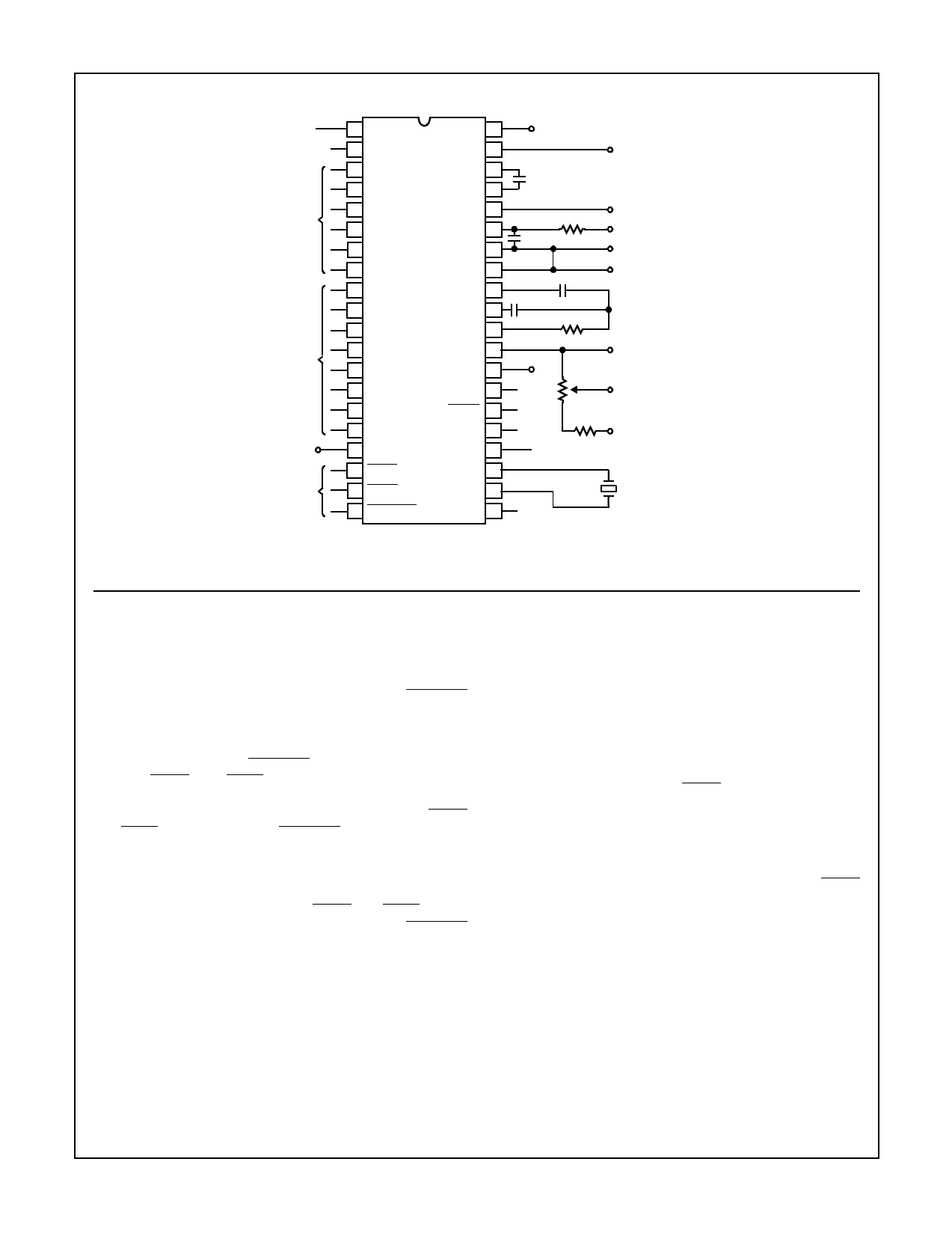
Test Circuit
ICL7109
GND
HIGH
ORDER
BYTE
OUTPUTS
LOW
ORDER
BYTE
OUTPUTS
+5V
BYTE
CONTROL
INPUTS
1 GND
V+ 40
+5V
2 STATUS REF IN - 39
-
3 POL
4 OR
REF CAP- 38
1µF
REF CAP+ 37
DIFFERENTIAL
REFERENCE
5 B12
6 B11
7 B10
REF IN+ 36
IN HI 35
IN LO 34
1MΩ R1
0.01µF
+
INPUT HIGH
INPUT LOW
8 B9
9 B8
10 B7
11 B6
12 B5
COMMON 33
INT 32
AZ 31
BUF 30
REF OUT 29
CINT
CAZ
0.15µF
0.33µF
RINT†
GND
REF IN -
13 B4
V- 28
-5V
14 B3
SEND 27
1kΩ
REF IN +
15 B2
RUN/HOLD 26
16 B1 BUF OSC OUT 25
17 TEST
OSC SEL 24
V+
GND 24kΩ
18 LBEN
19 HBEN
20 CE/LOAD
OSC OUT 23
OSC IN 22
3.5795MHz
TV CRYSTAL
MODE 21
†RINT = 20kΩ FOR 0.2V REF
= 200kΩ FOR 2.0V REF
Typical Applications
Direct Mode Interfacing
Figure 12 shows some of the combinations of chip enable
and byte enable control signals which may be used when
interfacing the ICL7109 to parallel data lines. The CE/LOAD
input may be tied low, allowing either byte to be controlled by
its own enable as in Figure 12A. Figure 12B shows a config-
uration where the two byte enables are connected together.
In this configuration, the CE/LOAD serves as a chip enable,
and the HBEN and LBEN may be connected to GND or
serve as a second chip enable. The 14 data outputs will all
be enabled simultaneously. Figure 12C shows the HBEN
and LBEN as flag inputs, and CE/LOAD as a master enable,
which could be the READ strobe available from most micro-
processors.
Figure 13 shows an approach to interfacing several
ICL7109s to a bus, connecting the HBEN and LBEN signals
of several converters together, and using the CE/LOAD
inputs (perhaps decode from an address) to select the
desired converter.
Some practical circuits utilizing the parallel three-state output
capabilities of the ICL7109 are shown in Figures 14 through
19. Figure 14 shows a straightforward application to the Intel
8048/80/85 microprocessors via an 8255PPI, where the
ICL7109 data outputs are active at all times. The I/O ports of
an 8155 may be used in the same way. This interface can be
used in a read-anytime mode, although a read performed
while the data latches are being updated will lead to
scrambled data. This will occur very rarely, in the proportion of
set-up skew times to conversion time. One way to overcome
this is to read the STATUS output as well, and if it is high, read
the data again after a delay of more than 1/2 converter clock
period. If STATUS is now low, the second reading is correct,
and if it is still high, the first reading is correct. Alternatively,
this timing problem is completely avoided by using a read-
after-update sequence, as shown in Figure 15. Here the high
to low transition of the STATUS output drives an interrupt to
the microprocessor causing it to access the data latches. This
application also shows the RUN/HOLD input being used to ini-
tiate conversions under software control.
A similar interface to Motorola MC6800 or Rockwell R650X
systems is shown in Figure 16. The high to low transition of
the STATUS output generates an interrupt via the Control
Register B CB1 line. Note that CB2 controls the RUN/HOLD
pin through Control Register B, allowing software-controlled
initiation of conversions in this system as well.
The three-state output capability of the ICL7109 allows direct
interfacing to most microprocessor busses. Examples of this
are shown in Figures 17 and 18. It is necessary to carefully
consider the system in this type of interface, to be sure that
requirements for setup and hold times, and minimum pulse
widths are met. Note also the drive limitations on long buses.
Generally this type of interface is only favored if the memory
peripheral address density is low so that simple address
decoding can be used. Interrupt handling can also require
many additional components, and using an interface device
will usually simplify the system in this case.
20
Share Link: 