PF28F1602C3TD70 Ver la hoja de datos (PDF) - Intel
NГәmero de pieza
componentes DescripciГіn
Fabricante
PF28F1602C3TD70 Datasheet PDF : 75 Pages
| |||
C3 SCSP Flash Memory
2.0
Principles of Operation
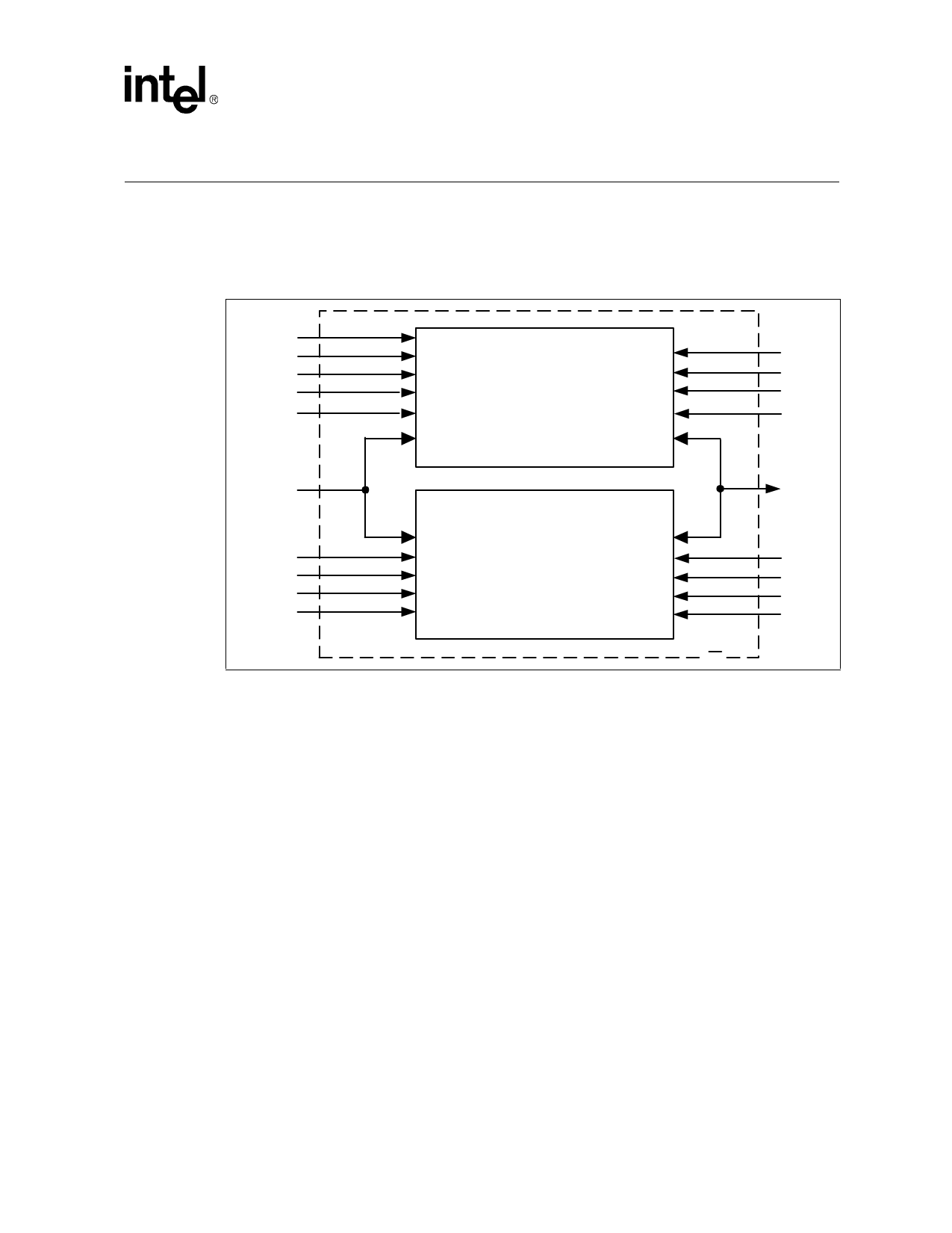
Figure 2.
The flash memory uses a CUI and automated algorithms to simplify program and erase operations.
To automate program and erase operations, the WSM handles data and address latches, WE#, and
system status requests.
IntelВ® Advanced+ Boot Block SCSP Block Diagram
F-VCC
F-OE#
F-CE#
F-WP#
F-RP#
Flash
28F160C3
or
28F320C3
F-VCCQ
F-WE#
F-VPP
F-VSS
A[Max:0]
S-VCC
S-CS1
S-CS2
S-OE#
SRAM
2-, 4- or 8-Mbit
D[15:0]
S-VSS
S-WE#
S-UB#
S-LB#
.
2.1
Bus Operation
All bus cycles to or from the SCSP conform to standard microcontroller bus cycles. Four control
signals dictate the data flow in and out of the flash component:
вҖў F-CE#
вҖў F-OE#
вҖў F-WE#
вҖў F-RP#
Four separate control signals handle the data flow in and out of the SRAM component:
вҖў S-CS1#
вҖў S-CS2
вҖў S-OE#
вҖў S-WE#
Table 2 on page 9 and Table 3 on page 12 summarize these bus operations .
Datasheet
IntelВ® Advanced+ Boot Block Flash Memory (C3) SCSP Family
Order Number: 252636, Revision: 004
26 Aug 2005
11
Share Link: 