PF28F1602C3TD70 Ver la hoja de datos (PDF) - Intel
NĂşmero de pieza
componentes DescripciĂłn
Fabricante
PF28F1602C3TD70 Datasheet PDF : 75 Pages
| |||
C3 SCSP Flash Memory
2.1.1
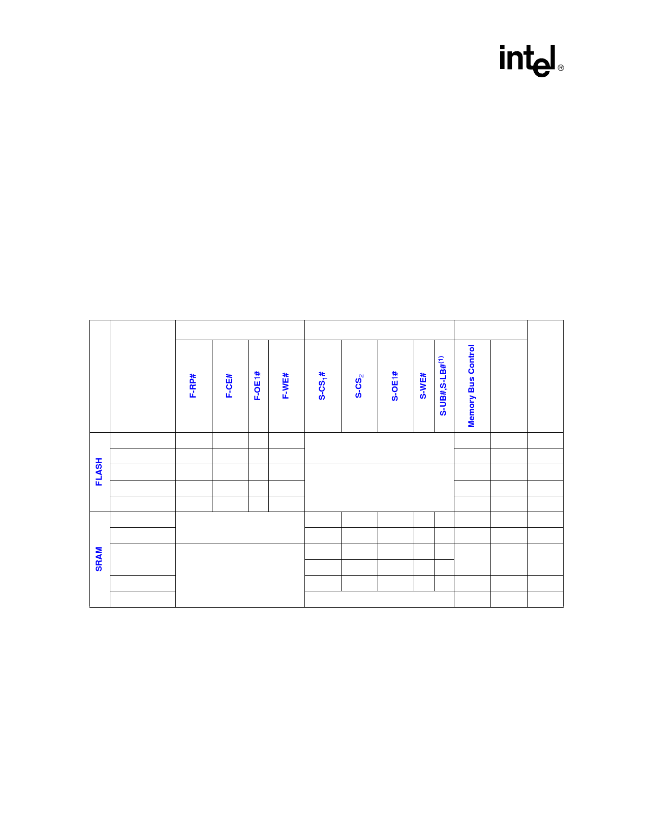
Table 3.
Read
The flash memory device provides four read modes:
⢠Read array
⢠Read identifier
⢠Read status
⢠CFI query
These flash memory read modes do not depend on the F-VPP voltage. Upon initial device power-up
or after exit from reset, the flash memory device automatically defaults to read array mode. F-CE#
and F-OE# must be asserted to obtain data from the flash memory device.
The SRAM provides only one read mode. S-CS1#, S-CS2, and S-OE# must be asserted to obtain
data from the SRAM device. See Table 3 for a summary of operations.
Intel Advanced+ Boot Block Flash Memory SCSP Bus Operations
Flash Signals
SRAM Signals
Memory Output
Modes
D0â Notes
D15
Read
Write
Standby
H
L
L
H
H
L
H
L
H
H
X
X
SRAM must be in High Z
Flash
Flash
Other
DOUT
DIN
High Z
Output Disable H
L
H
H
Any SRAM mode is allowable
Other High Z
Reset
L
X
X
X
Other High Z
Read
Write
FLASH must be in High Z
L
H
L
H L SRAM DOUT
L
H
H
L L SRAM DIN
H
X
X
XX
Standby
Other High Z
X
L
X
XX
Any FLASH mode is allowable
Output Disable
L
H
H
H X Other High Z
Data Retention
same as a standby
Other High Z
Notes:
1.
Two devices cannot drive the memory bus at the same time.
2.
To place the SRAM into data retention mode, lower the S-VCC signal to the VDR range, as specified.
2,3,4
2,4
5,6
5,6
5,6
2,4
2,4
4,5,6
4,5,6
4,5,7
2.1.2
Output Disable
When F-OE# and S-OE# are deasserted, the SCSP output signals are placed in a high-impedance
state.
26 Aug 2005
12
IntelÂŽ Advanced+ Boot Block Flash Memory (C3) SCSP Family
Order Number: 252636, Revision: 004
Datasheet
Share Link: 