GT28F400B3B150 Ver la hoja de datos (PDF) - Intel
Número de pieza
componentes Descripción
Fabricante
GT28F400B3B150 Datasheet PDF : 49 Pages
| |||
E
SMART 3 ADVANCED BOOT BLOCK–WORD-WIDE
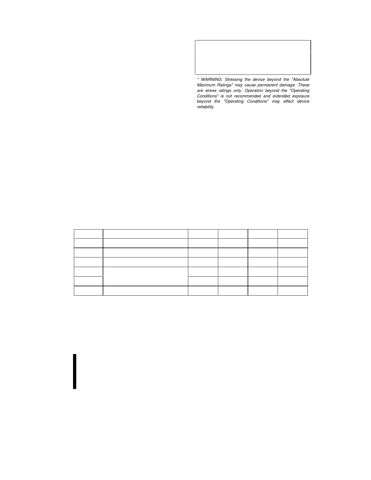
4.0 ABSOLUTE MAXIMUM
RATINGS*
Extended Operating Temperature
During Read ............................ –40°C to +85°C
During Block Erase
and Program............................ –40°C to +85°C
Temperature Under Bias ......... –40°C to +85°C
Storage Temperature................... –65°C to +125°C
Voltage on Any Pin
(except VCC, VCCQ and VPP)
with Respect to GND ............... –0.5V to +5.0V1
VPP Voltage (for Block
Erase and Program)
with Respect to GND .........–0.5V to +13.5V1,2,4
VCC and VCCQ Supply Voltage
with Respect to GND ............... –0.2V to +5.0V1
Output Short Circuit Current...................... 100 mA3
NOTICE: This datasheet contains preliminary information on
new products in production. Do not finalize a design with
this information. Revised information will be published when
the product is available. Verify with your local Intel Sales
office that you have the latest data sheet before finalizing a
design.
* WARNING: Stressing the device beyond the "Absolute
Maximum Ratings" may cause permanent damage. These
are stress ratings only. Operation beyond the "Operating
Conditions" is not recommended and extended exposure
beyond the "Operating Conditions" may effect device
reliability.
NOTES:
1. Minimum DC voltage is –0.5V on input/output pins.
During transitions, this level may undershoot to –2.0V
for periods < 20 ns. Maximum DC voltage on
input/output pins is VCC + 0.5V which, during
transitions, may overshoot to VCC + 2.0V for periods <
20 ns.
2. Maximum DC voltage on VPP may overshoot to +14.0V
for periods < 20 ns.
3. Output shorted for no more than one second. No more
than one output shorted at a time.
4. VPP Program voltage is normally 2.7V–3.6V.
Connection to supply of 11.4V–12.6V can only be done
for 1000 cycles on the main blocks and 2500 cycles on
the parameter blocks during program/erase. VPP may
be connected to 12V for a total of 80 hours maximum.
See Section 3.4 for details.
5.0 OPERATING CONDITIONS (VCCQ = 2.7V–3.6V)
Table 9. Temperature and Voltage Operating Conditions4
Symbol
Parameter
Notes
Min
Max
Units
TA
VCC
VCCQ
VPP1
Operating Temperature
2.7V–3.6V VCC Supply Voltage
2.7V–3.6V I/O Supply Voltage
Program and Erase Voltage
–40
1,4
2.7
1,2,4
2.7
4
2.7
+85
°C
3.6
Volts
3.6
Volts
3.6
Volts
VPP2
3
11.4
12.6
Volts
Cycling
Block Erase Cycling
5
10,000
Cycles
NOTES:
1. See DC Characteristics tables for voltage range-specific specifications.
2. The voltage swing on the inputs, VIN is required to match VCCQ.
3. Applying VPP = 11.4V–12.6V during a program/erase can only be done for a maximum of 1000 cycles on the main blocks
and 2500 cycles on the parameter blocks. VPP may be connected to 12V for a total of 80 hours maximum. See Section 3.4
for details.
4. VCC, VCCQ and VPP1 must share the same supply when all three are between 2.7V and 3.6V.
5. For operating temperatures of –25°C– +85°C the device is projected to have a minimum block erase cycling of 10,000 to
30,000 cycles.
PRELIMINARY
29
Share Link: 