GT28F400B3B150 Ver la hoja de datos (PDF) - Intel
Número de pieza
componentes Descripción
Fabricante
GT28F400B3B150 Datasheet PDF : 49 Pages
| |||
SMART 3 ADVANCED BOOT BLOCK–WORD-WIDE
E
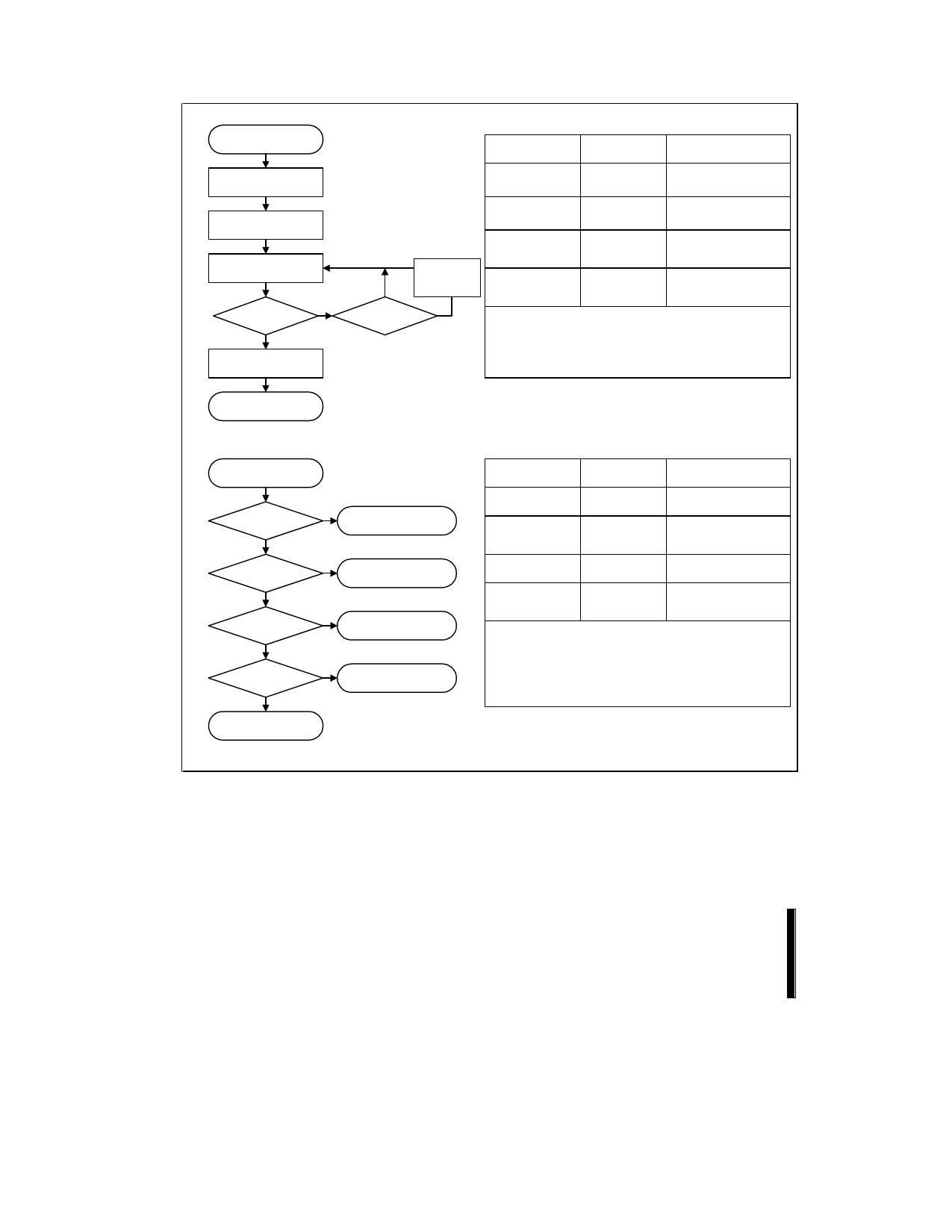
Start
Write 20H
Write D0H and
Block Address
Read Status Register
0
SR.7 =
1
Full Status
Check if Desired
Bus Operation
Command
Comments
Write
Write
Erase Setup
Erase Confirm
Read
Suspend
Erase Loop
No
Yes
Suspend Erase
Standby
Repeat for subsequent block erasures.
Data = 20H
Addr = Within Block to Be
Erased
Data = D0H
Addr = Within Block to Be
Erased
Status Register Data Toggle
CE# or OE# to Update Status
Register Data
Check SR.7
1 = WSM Ready
0 = WSM Busy
Full Status Check can be done after each block erase or after a sequence of
block erasures.
Write FFH after the last write operation to reset device to read array mode.
Block Erase Complete
FULL STATUS CHECK PROCEDURE
Read Status Register
Data (See Above)
SR.3 =
1
VPP Range Error
0
SR.4,5 =
0
SR.5 =
1
Command Sequence
Error
1
Block Erase Error
0
SR.1 =
0
Block Erase
Successful
1
Attempted Erase of
Locked Block - Aborted
Bus Operation
Command
Comments
Standby
Standby
Check SR.3
1 = VPP Low Detect
Check SR.4,5
Both 1 = Command Sequence
Error
Standby
Check SR.5
1 = Block Erase Error
Standby
Check SR.1
1 = Attempted Erase of
Locked Block - Erase Aborted
SR. 1 and 3 MUST be cleared, if set during an erase attempt, before further
attempts are allowed by the Write State Machine.
SR.1, 3, 4, 5 are only cleared by the Clear Staus Register Command, in cases
where multiple bytes are erased before full status is checked.
If an error is detected, clear the status register before attempting retry or other
error recovery.
0580_09
Figure 9. Automated Block Erase Flowchart
24
PRELIMINARY
Share Link: 