DS80C400 Ver la hoja de datos (PDF) - Dallas Semiconductor -> Maxim Integrated
Número de pieza
componentes Descripción
Fabricante
DS80C400 Datasheet PDF : 10 Pages
| |||
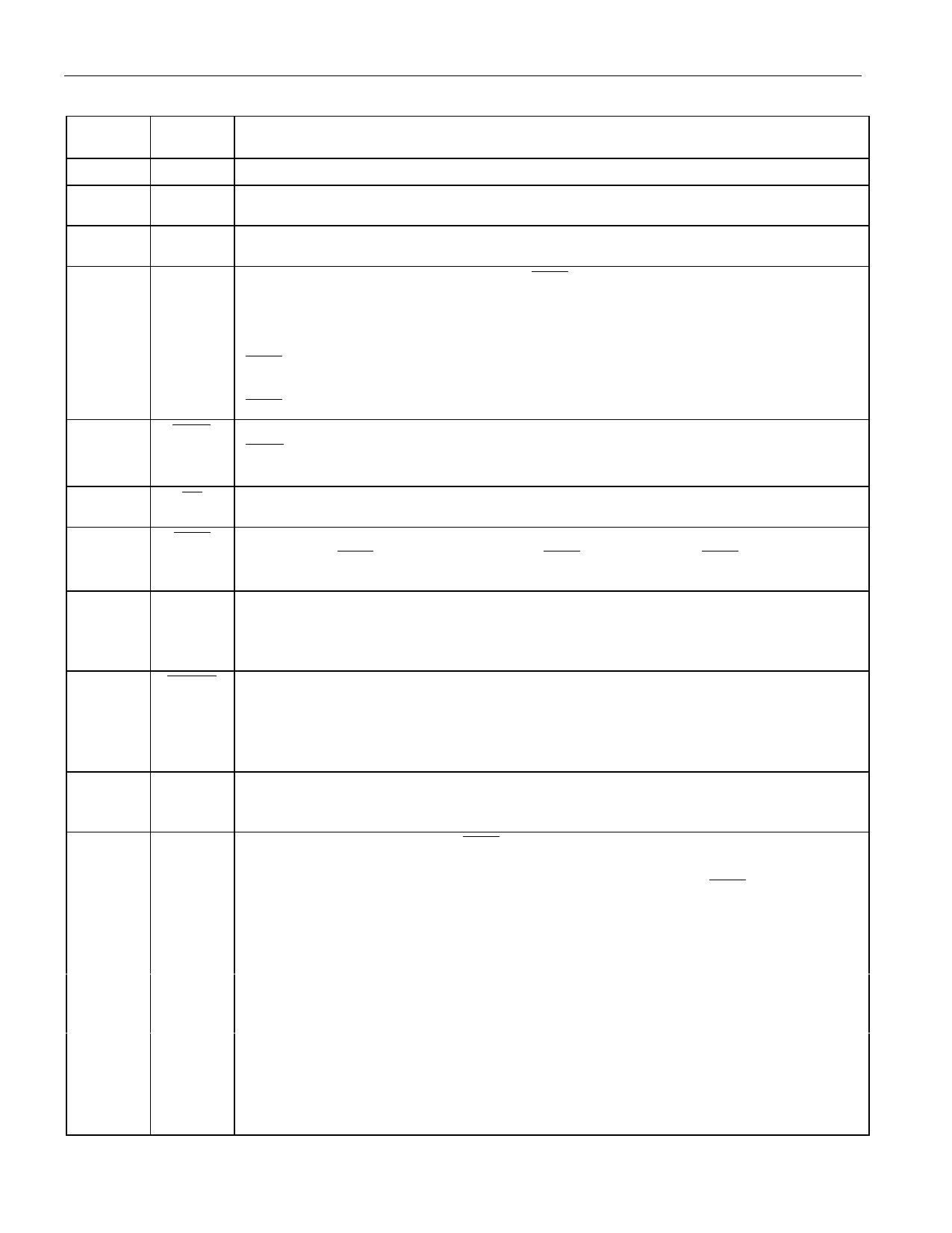
Table 1. Pin Description
DS80C400
PIN
70
12, 36,
62, 87
13, 39,
63, 88
68
67
69
40
97
98
37,
38
86
85
84
83
82
81
80
79
NAME
FUNCTION
VCC1
VCC3
+1.8V Core Supply Voltage
+3.3V I/O Supply Voltage
VSS
ALE
PSEN
EA
MUX
RST
RSTOL
XTAL2,
XTAL1
Digital Circuit Ground
Address Latch Enable, Output. When the MUX pin is low, this pin outputs a clock to
latch the external address LSB from the multiplexed address/data bus on Port 0. This
signal is commonly connected to the latch enable of an external transparent latch. ALE
has a pulse width of 1.5 XTAL1 cycles and a period of four XTAL1 cycles. When the
MUX pin is high, the pin toggles continuously if the ALEOFF bit is cleared. ALE is
forced high when the device is in a reset condition or if the ALEOFF bit is set while the
MUX pin is high.
Program Store Enable, Output. This signal is the chip enable for external ROM memory.
PSEN provides an active-low pulse and is driven high when external ROM is not being
accessed.
External Access Enable, Input. Connect to GND to use external program memory.
Connect to VCC to use internal ROM.
Multiplex/Demultiplex Select, Input. This pin selects if the address/data bus operates in
multiplexed ( MUX = 0) or demultiplexed ( MUX = 1) mode. The MUX pin is sampled
only on a power-on reset.
Reset, Input. The RST input pin contains a Schmitt voltage input to recognize external
active-high reset inputs. The pin also employs an internal pulldown resistor to allow for a
combination of wired-OR external-reset sources. An RC circuit is not required for power-
up, as the device provides this function internally.
Reset Output Low, Output. This active-low signal is asserted:
when the microcontroller has entered reset through the RST pin; during crystal warm-up
period following power-on or stop mode; during a watchdog timer reset (2 cycles
duration); during an oscillator failure (if OFDE = 1); whenever VCC1 £ VRST1 or VCC3 £
VRST3
XTAL1, XTAL2. Crystal oscillator pins support fundamental mode, parallel resonant, AT
cut crystals. XTAL1 is the input if an external clock source is used in place of a crystal.
XTAL2 is the output of the crystal amplifier.
AD0–7 (Port 0), I/O. When the MUX pin is connected low, Port 0 is the multiplexed
address/data bus. While ALE is high, the LSB of a memory address is presented. While
ALE falls, the port transitions to a bidirectional data bus. When the MUX pin is
connected high, Port 0 functions as the bidirectional data bus. Port 0 cannot be modified
by software. The reset condition of Port 0 pins is high. No pullup resistors are needed.
Port
AD0/D0 P0.0
AD1/D1 P0.1
AD2/D2 P0.2
AD3/D3 P0.3
AD4/D4 P0.4
AD5/D5 P0.5
AD6/D6 P0.6
AD7/D7 P0.7
Alternate Function
AD0/D0 (Address)/Data 0
AD1/D1 (Address)/Data 1
AD2/D2 (Address)/Data 2
AD3/D3 (Address)/Data 3
AD4/D4 (Address)/Data 4
AD5/D5 (Address)/Data 5
AD6/D6 (Address)/Data 6
AD7/D7 (Address)/Data 7
4 of 125
Share Link: 