1EDI2004AS Ver la hoja de datos (PDF) - Infineon Technologies
Número de pieza
componentes Descripción
Fabricante
1EDI2004AS Datasheet PDF : 138 Pages
| |||
EiceDRIVERTM SIL
1EDI2004AS
Specification
5.2
Absolute Maximum Ratings
Stress above the maximum values listed here may cause permanent damage to the device. Exposure to
absolute maximum rating conditions for extended periods may affect device reliability.
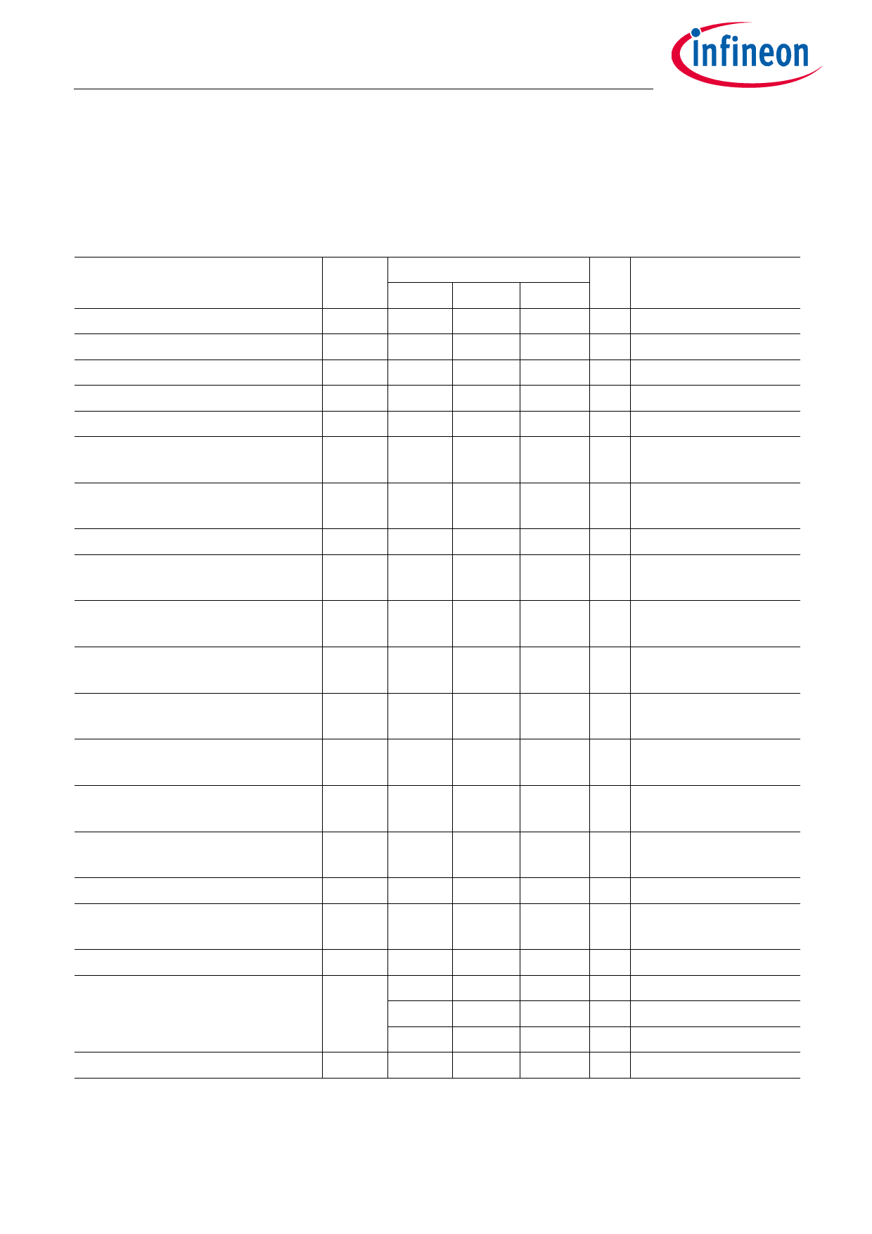
Table 40 Absolute Maximum Ratings1)
Parameter
Symbol
Values
Unit Note or Test Condition
Min. Typ. Max.
Junction temperature
TJUNC -40
-
Storage temperature
TSTO
-55
-
Positive power supply (primary)
VCC1MAX -0.3
-
Positive power supply (secondary) VCC2MAX -0.3
-
Negative power supply
VEE2MAX -13
-
Power supply voltage difference
VDS2
-
-
(secondary) VCC2-VEE2
Voltage on any I/O pin on prim. side VIN1
-0.3
-
except INP, INSTP, EN
Voltage on INP, INSTP, EN pins
VINR1
-0.3
-
Voltage difference between REF0 VDG1 -4
-
and GND1
150
°C
150
°C
6.0
V Referenced to GND1
28
V Referenced to GND2
0.3
V Referenced to GND2
40
V
6.0
V Referenced to GND1
6.0
V Referenced to REF02)
4
V
Voltage difference between OCPG VOCPG2 -0.3
-
and GND2
0.3
V
TON & TOFF Source / Sink Peak
I15O2MAX -
-
2.7
A VCC2=18V, VEE2=-10V,
Current
max. pulse tMAX = 3.5µs
Output current on push-pull I/O on IOUTPP1 -
-
20
mA
primary side
Output current on push-pull I/O on IOUTPP2 -
-
20
mA
secondary side
Output current on open drain I/O on IOUTOD1 -
-
20
mA
primary side
Output current on open drain I/O on IOUTOD2 -
-
10
mA
secondary side
Voltage on 5 V pin on secondary side. VIN52
Voltage on 15 V pin on secondary
side.
VIN152
-0.3 -
VEE2-0.3 -
6.0
V
VCC2+0.3 V
Referenced to GND2
Referenced to GND2,
except DESAT
Voltage on DESAT pin.
ESD Immunity
VINDESAT -0.3
-
VESD
-
-
-
-
20
V Referenced to GND2
2
kV HBM3)
750
V CDM4), pins 1, 16, 17, 36
500
V CDM4), all other pins
MSL Level
MSL n.a. 3
n.a.
1) Not subject to production test. Absolute maximum Ratings are verified by design / characterization.
2) Max. voltage of VINR1+VDG1 should be below 7V.
3) According to EIA/JESD22-A114-B.
4) According to JESD22-C101-C.
Data Sheet
121
Rev. 2.0
2019-01-16
Share Link: 