RD28F1602C3B110_03 Ver la hoja de datos (PDF) - Intel
NГәmero de pieza
componentes DescripciГіn
Fabricante
RD28F1602C3B110_03
Intel

RD28F1602C3B110_03 Datasheet PDF : 70 Pages
| |||
3 Volt IntelВ® Advanced+ Boot Block Flash Memory Stacked-CSP Family
2.0
Principles of Operation
The flash memory utilizes a CUI and automated algorithms to simplify program and erase
operations. The WSM automates program and erase operations by handling data and address
latches, WE#, and system status requests.
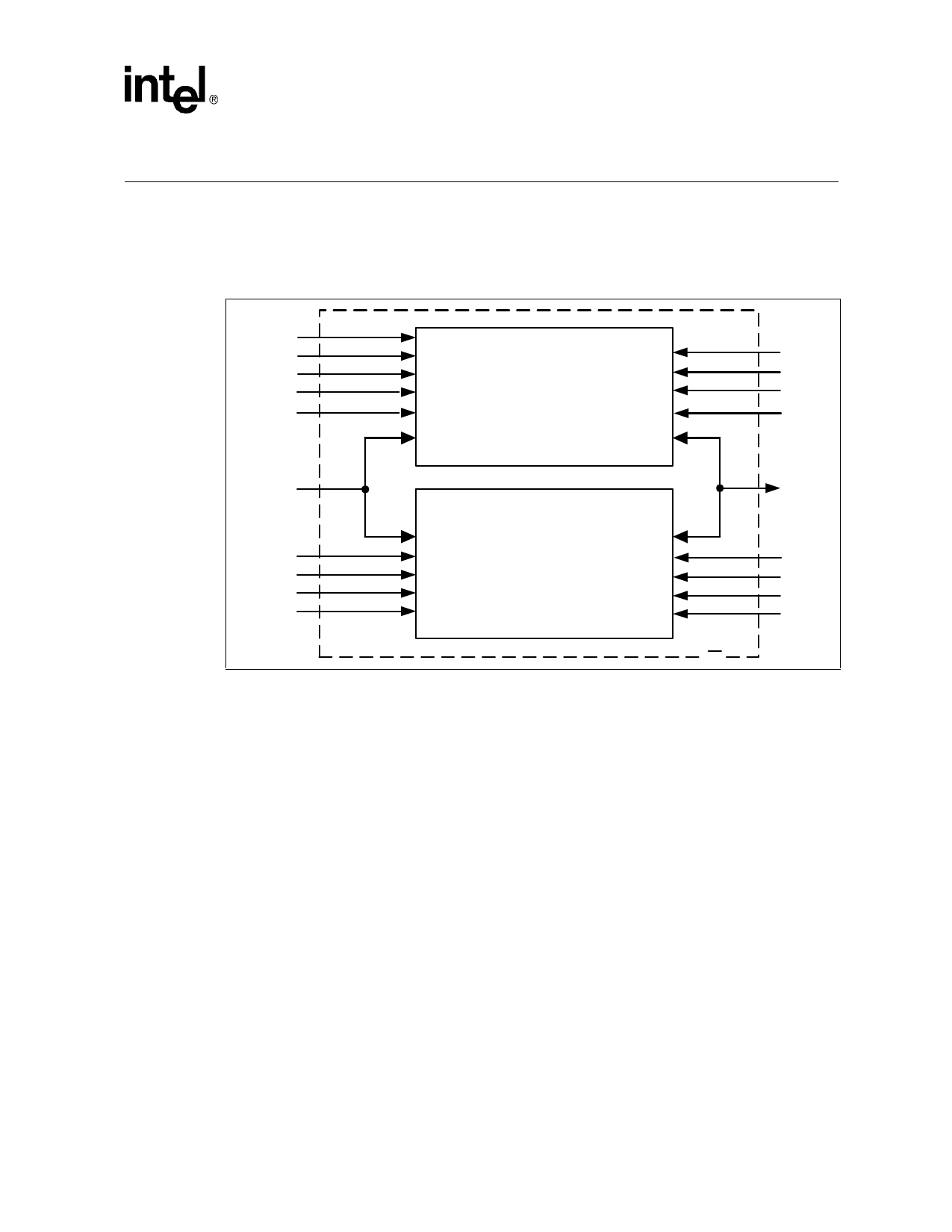
Figure 2. 3 Volt IntelВ® Advanced+ Boot Block Stacked Chip Scale Package Block Diagram
F-VCC
F-OE#
F-CE#
F-WP#
F-RP#
Flash
28F160C3
or
28F320C3
F-VCCQ
F-WE#
F-VPP
F-VSS
A[Max:0]
S-VCC
S-CS1
S-CS2
S-OE#
SRAM
2-, 4- or 8-Mbit
D[15:0]
S-VSS
S-WE#
S-UB#
S-LB#
.
2.1
2.1.1
Bus Operation
All bus cycles to or from the Stacked-CSP conform to standard microcontroller bus cycles. Four
control signals dictate the data flow in and out of the flash component: F-CE#, F-OE#, F-WE# and
F-RP#. Four separate control signals handle the data flow in and out of the SRAM component:
S-CS1#, S-CS2, S-OE#, and S-WE#. These bus operations are summarized in Table 2 and Table 3.
Read
The flash memory has four read modes: read array, read identifier, read status and CFI query. These
flash memory read modes are not dependent on the F-VPP voltage. Upon initial device power-up or
after exit from reset, the flash device automatically defaults to read array mode. F-CE# and F-OE#
must be asserted to obtain data from the flash component.
The SRAM has one read mode available. S-CS1#, S-CS2, and S-OE# must be asserted to obtain
data from the SRAM device. See Table 3, вҖң3 Volt Intel Advanced+ Boot Block Flash Memory
Stacked-CSP Bus OperationsвҖқ on page 12 for a summary of operations.
Datasheet
11
Share Link: