BD6369GUL Ver la hoja de datos (PDF) - ROHM Semiconductor
Número de pieza
componentes Descripción
Fabricante
BD6369GUL Datasheet PDF : 17 Pages
| |||
BD6883GUL,BH6453GUL,BD6886GUL,BD6369GUL
Technical Note
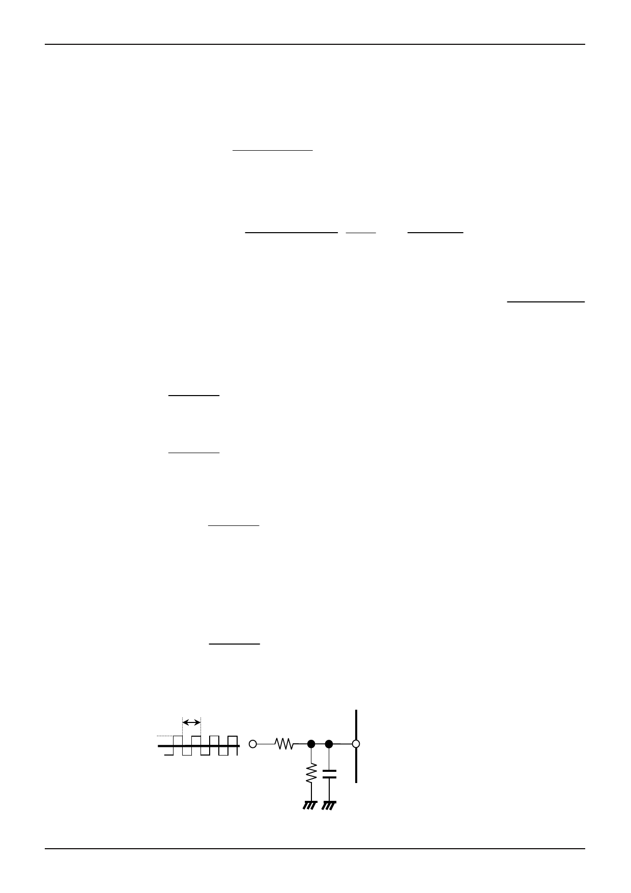
7) Setting of PWM signal input VLIM and CLIM terminals (all series)
It is also possible to compose filters outside the IC, change an input voltage for output voltage and output current setting terminals
such as VLIM and CLIM terminals by the DUTY control using an PWM signal, etc., and use them as set values for control.
In this case, however, ensure the smoothing of the signals, heeding the constant number of the low-pass filter as stated below.
A cutoff frequency FC (-3dB attenuation frequency) of the low-pass filter in Fig25 is calculated by the formula mentioned below.
Cutoff frequency FC [Hz] =
1
[Hz]
2πCIN (RINA//RINB)
・・・・・④
Set the cutoff frequency FC at 1/100 or below of the PWM frequency FPWM.
For example, if the cutoff frequency FC is set at 1/100 of FPWM when the PWM frequency FPWM=50[kHz], according to the formula
above:
Cutoff frequency FC [Hz] =
1
2πCIN (RINA//RINB)
= 1 ×FPWM= 50×103
100
100
[Hz]
・・・・・⑤
When CIN=0.1[μF], according to the formula above:
RINA//RINB=3.2[kΩ]
・・・・・⑥
ON time
Where, an effective value of PWM signal as a DC current, according to crest values VMAX and ON DUTY [%]= ON time+ OFF time
is as follows:
VPWM[V]= VMAX[V]× ON DUTY[%]
・・・・・⑦
An actual voltage VLIM input to terminals that specify output current and voltages, such as VLIM and CLIM terminals
is as follows according to resistance potential division of RINA and RINB:
VLIM[V]=
RINB
RINA+RINB
×VPWM[V]
・・・・・⑧
For example, when an PWM signal with crest values VMAX=3[V] and DUTY [%]=5[%] is input, a VLIM value according to the formula
above is:
VLIM[V]=
RINB
RINA+RINB
× 3[V]× 50[%]
・・・・・⑨
(Ⅰ)BD6883GUL, BD6886GUL, and BD6369GUL
Where, to specify an output voltage VOH=2[V], a value VLIM=1.0[V] according to the formula in the previous page. And then,
according to the formula above, VLIM=1.0[V].
VLIM=1.0[V]=VLIM=
RINB
RINA+RINB
×3[V]×50[%]
Therefore, RINA=0.5RINB
⑩
According to ⑥ and ⑩, RINA=4.8kΩ, RINB=9.6kΩ.
・・・・・
(Ⅱ)BH6453GUL
Where, to specify an output current ISINK=100[mA], the following formula is derived according to the formula in the previous page
③, CLIM=0.4[V], and according to the formula above ⑨:
CLIM=0.4[V]=VLIM=
RINA=2.75RINB
RINB
RINA+RINB
×3[V]×50[%]
・・・・・⑪
According to ⑥ and ⑪: RINA=11.9kΩ, RINB=4.3kΩ
FPWM
VMAX
VPWM
RINA
VLIM Output voltage / Constant current voltage terminals
VLIM / CLIM
RINB
CIN
www.rohm.com
© 2012 ROHM Co., Ltd. All rights reserved.
Fig.25 Example PWM signal input
11/16
2012.03 - Rev.A
Share Link: 