LT8580 Ver la hoja de datos (PDF) - Linear Technology
Número de pieza
componentes Descripción
Fabricante
LT8580
LT8580 Datasheet PDF : 32 Pages
| |||

LT8580
Applications Information
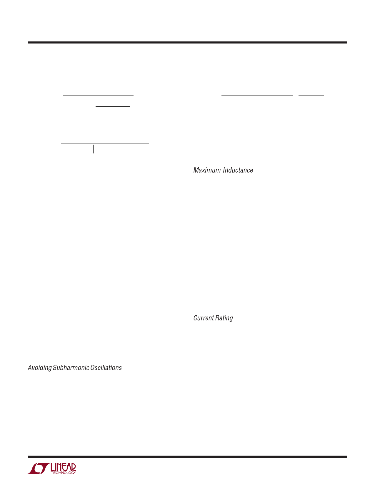
provided to a load (IOUT). In order to provide adequate
load current, L should be at least:
LBOOST
>
DC • VIN
2(f)
⎛
⎝⎜ILIM
−
|VOUT|
VIN
• IOUT
•h
⎞
⎟
⎠
for boost, topologies, or:
LDUAL
>
DC • VIN
⎛
2(f) ⎜ILIM−
⎝
VOUT
VIN
• IOUT
•h
⎞
−
IOUT
⎟
⎠
for the SEPIC and inverting topologies.
where:
LBOOST = L1 for boost topologies (see Figure 15)
LDUAL = L1 = L2 for coupled dual inductor topologies
(see Figure 16 and Figure 17)
LDUAL = L1||L2 for uncoupled dual inductor topologies
(see Figure 16 and Figure 17)
DC = switch duty cycle (see previous section)
ILIM = switch current limit, typically about 1.2A at 50%
duty cycle (see the Typical Performance Characteristics
section).
h = power conversion efficiency (typically 85% for boost
and 83% for dual inductor topologies at high currents).
f = switching frequency
IOUT = maximum load current
Negative values of L indicate that the output load current
IOUT exceeds the switch current limit capability of the
LT8580.
Avoiding Subharmonic Oscillations: The LT8580’s internal
slope compensation circuit can prevent subharmonic oscil-
lations that can occur when the duty cycle is greater than
50%, provided that the inductance exceeds a minimum
value. In applications that operate with duty cycles greater
than 50%, the inductance must be at least:
LMIN
>
VIN
1.25 • (DC − 300nS
•
f)
•
f
2 DC − 1
1− DC
LMIN = L1 for boost topologies (see Figure 15)
LMIN = L1 = L2 for coupled dual inductor topologies
(see Figure 16 and Figure 17)
LMIN = L1||L2 for uncoupled dual inductor topologies
(see Figure 16 and Figure 17)
Maximum Inductance: Excessive inductance can reduce
current ripple to levels that are difficult for the current com-
parator (A3 in the Block Diagram) to cleanly discriminate,
thus causing duty cycle jitter and/or poor regulation. The
maximum inductance can be calculated by:
LMAX
=
VIN − VCESAT
IMIN-RIPPLE
•
DC
f
where
LMIN = L1 for boost topologies (see Figure 15)
LMIN = L1 = L2 for coupled dual inductor topologies
(see Figure 16 and Figure 17)
LMIN = L1||L2 for uncoupled dual inductor topologies
(see Figure 16 and Figure 17)
IMIN(RIPPLE) = typically 80mA
Current Rating: Finally, the inductor(s) must have a rating
greater than its peak operating current to prevent inductor
saturation resulting in efficiency loss. In steady state, the
peak input inductor current (continuous conduction mode
only) is given by:
IL1-PEAK
=
|VOUT • IOUT|
VIN • h
+
VIN • DC
2 • L1• f
for the boost, uncoupled inductor SEPIC and uncoupled
inductor inverting topologies.
For more information www.linear.com/LT8580
8580f
11