LT8580 Ver la hoja de datos (PDF) - Linear Technology
Número de pieza
componentes Descripción
Fabricante
LT8580
Linear Technology

LT8580 Datasheet PDF : 32 Pages
| |||
LT8580
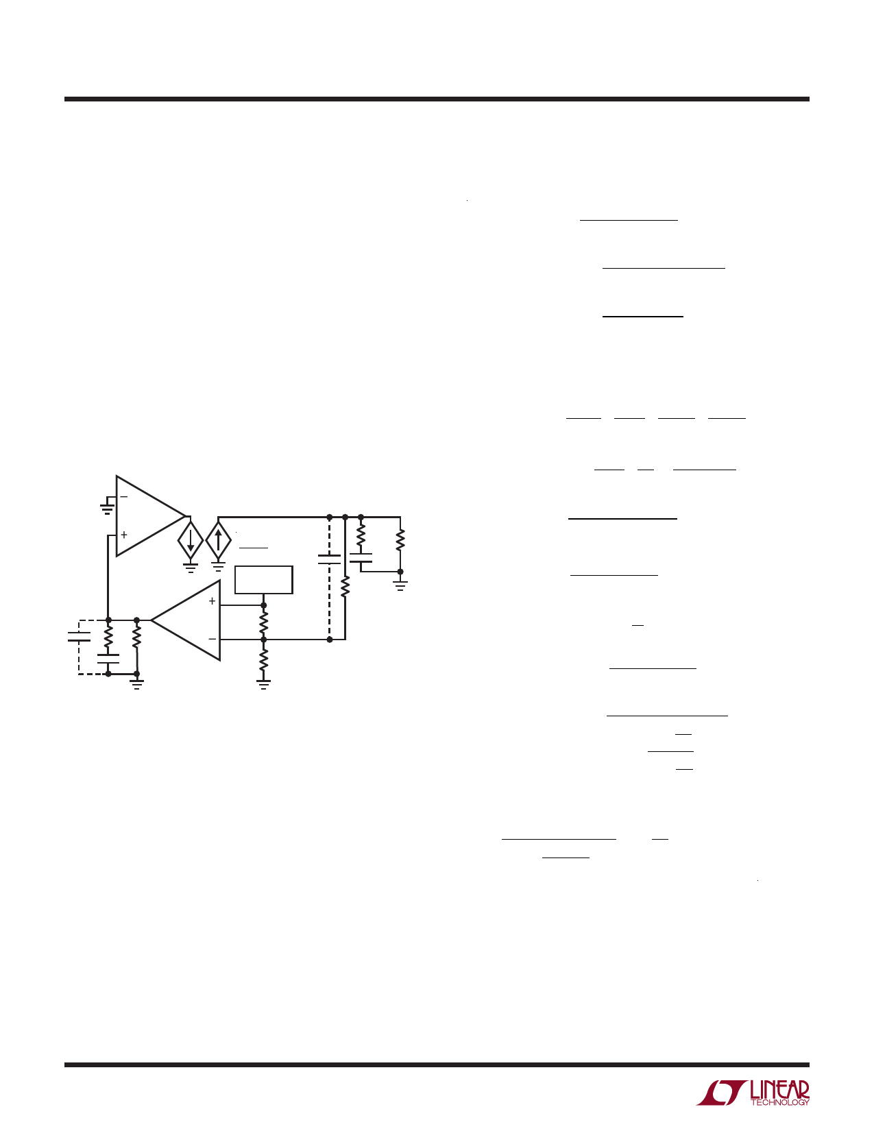
Applications Information
As with any feedback loop, identifying the gain and phase
contribution of the various elements in the loop is critical.
Figure 5 shows the key equivalent elements of a boost con-
verter. Because of the fast current control loop, the power
stage of the IC, inductor and diode have been replaced by
a combination of the equivalent transconductance ampli-
fier gmp and the current controlled current source which
converts IVIN to (ηVIN/VOUT) • IVIN. gmp acts as a current
source where the peak input current, IVIN, is proportional
to the VC voltage. η is the efficiency of the switching
regulator, and is typically about 85%.
Note that the maximum output currents of gmp and gma are
finite. The limits for gmp are in the Electrical Characteristics
section (switch current limit), and gma is nominally limited
to about +15µA and –17µA.
–
gmp
+
VC
CF RC RO
CC
IVIN
gma
η • VIN
VOUT
• IVIN
CPL
1.204V
REFERENCE
R2
FBX
R2
VOUT
RESR
RL
COUT
R1
8580 F05
CC: COMPENSATION CAPACITOR
COUT: OUTPUT CAPACITOR
CPL: PHASE LEAD CAPACITOR
CF: HIGH FREQUENCY FILTER CAPACITOR
gma: TRANSCONDUCTANCE AMPLIFIER INSIDE IC
gmp: POWER STAGE TRANSCONDUCTANCE AMPLIFIER
RC: COMPENSATION RESISTOR
RL: OUTPUT RESISTANCE DEFINED AS VOUT DIVIDED BY ILOAD(MAX)
RO: OUTPUT RESISTANCE OF gma
R1, R2: FEEDBACK RESISTOR DIVIDER NETWORK
RESR: OUTPUT CAPACITOR ESR
η: CONVERTER EFFICIENCY (~85% AT HIGHER CURRENTS)
Figure 5. Boost Converter Equivalent Model
From Figure 5, the DC gain, poles and zeros can be cal-
culated as follows:
Output Pole: P1=
2
2 • π • RL • COUT
Error Amp Pole: P2 =
1
2 • π • [RO +RC ] • CC
Error Amp Zero: Z1=
1
2 • π • RC • CC
DC Gain:
(Breaking Loop at FBX Pin)
ADC
= AOL(0) =
∂VC
∂VFBX
•
∂IVIN
∂VC
•
∂VOUT
∂IVIN
•
∂VFBX =
∂VOUT
(gma
•
R0
)
•
gmp
•
⎛
⎜h
⎝
•
VIN
VOUT
• RL
2
⎞
⎟•
⎠
0.5R2
R1+ 0.5R2
ESR Zero: Z2 =
1
2 • π • RESR • COUT
RHP Zero:
Z3
=
4
•
VI2N
π•
• RL
VO2UT
•
L
High Frequency Pole: P3 > fS
3
Phase Lead Zero: Z4 =
1
2 • π • R1• CPL
Phase Lead Pole: P4 =
1
R1• R2
2
•
π
•
R1+
2
R2
•
CPL
2
Error Amp Filter Pole:
P5
=
2•π
•
1
RC • RO
RC + RO
, CF
• CF
< CC
10
The current mode zero (Z3) is a right-half plane zero
which can be an issue in feedback control design, but is
manageable with proper external component selection.
8580f
14
For more information www.linear.com/LT8580
Share Link: