RT9206 Ver la hoja de datos (PDF) - Richtek Technology
Número de pieza
componentes Descripción
Fabricante
RT9206 Datasheet PDF : 21 Pages
| |||
RT9206
iS1
VIN
S1
S2
d
-
+
PWM
Generator
L
iL
+ VL -
iS2
+
VOR
-
+
VOC
-
iC
rC
RL
COUT
IOUT
+
VOUT
-
Compensator
VREF
Sensor
Gain
Ra
VC
Cc2
gm+
-
Rc1
Cc1
Rb
Next, deriving the transfer function d(s)/vC (s) of the direct
duty ratio pulse-width modulator (PWM Generator). The
transfer function Tm(s) of the modulator is given by
Tm(S) = d(S) = 1
VC(S) Vr
(19)
where, Vr is the amplitude of ramp-waveform which is listed
in datasheet.
For simplification, the transfer function of PWM generator
and Buck converter can is combined. The resulting is shown
in equation (20)
G(S)
=
VOUT(S)
VC(S)
=
S2
xL
1+ rc x CO x S
+ CO x S( L + rc
x
x
CO) + 1
V IN
Vr
RL
(20)
The transfer function of Equation (20) is a second order
system and Bode plot is shown in Figure 7.
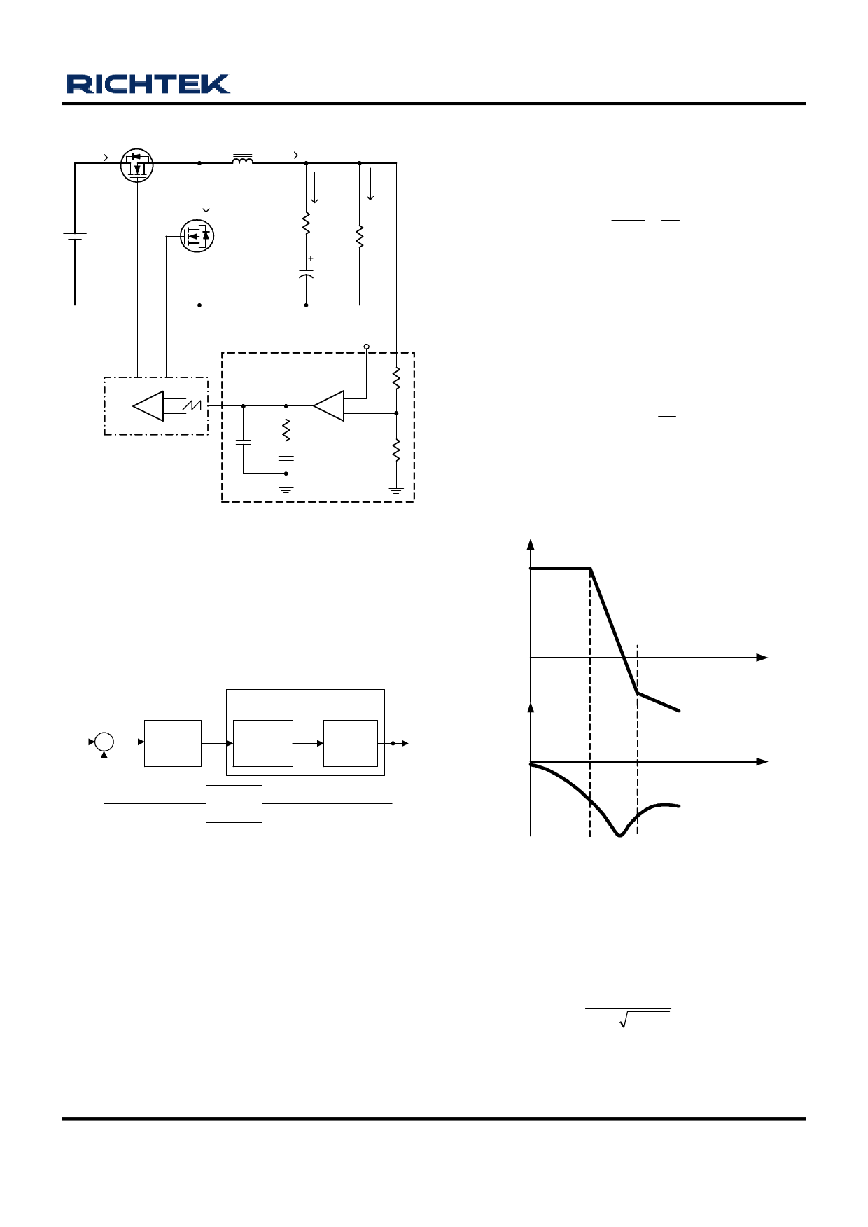
Figure 5. The simplified diagram for synchronous Buck
converter and control loop.
Gain
VIN/Vr
From control system point of view, the block diagram of
Figure 5 is shown in Figure 6.
VREF +
-
Compensator
C(s) Vc(s)
G(S)
PWM
Generator
BUCK
Converter
1/Vr d(s) Gp(s)
VOUT
Rb H (s)
Ra+Rb
Sensor Gain
Figure 6. The control block diagram of synchronous
Buck converter
f
fp
fz
Phase
0°
f
-90°
-180°
Figure 7. The Bode plot of Buck power stage
First, deriving the accurate small-signal models of power
stage, the equation (18) is the transfer function of
vO(s)/d(s), which be obtained by space averaging
technique.
GP(S)
=
VOUT(S)
d(S)
=
S2
x
L
1+ rc x CO x S
x CO + S( L + rc
x
CO)
+1
x
VIN
RL
(18)
In Figure 7, the resonance of the output LC filter produces
a double pole and −40dB/decade slop. The resonance
frequency is expressed as follows :
fP =
1
2π x L x CO
(Hz) (21)
DS9206-11 March 2007
www.richtek.com
17
Share Link: 