RT9206 Ver la hoja de datos (PDF) - Richtek Technology
Número de pieza
componentes Descripción
Fabricante
RT9206 Datasheet PDF : 21 Pages
| |||
RT9206
The MOSFET should be capable of handling the power
loss over the entire operating range.
Design Example:
Design the power stage for a synchronous step-down
converter having the following specifications:
VIN = 12V, VOUT = 5V, IOUT = 5A, ∆VOUT < 25mV, switching
frequency = 200kHz, to determine the value of inductor
and output capacitor (Using electrolytic capacitor).
First, select ripple current of inductor is 20% of output
current, from equation (1)
5
L = (12 - 5) ×
= 14.58µH
12 × 200K × 0.2 × 5
Select L = 15µH
From equation (5)
25mV=1 x rC
Select two electrolytic capacitors C = 470µF,rC = 43mΩ
in parallel.
Setting the Current Limit
The RT9206 limits output current by sensing low side
MOSFET voltage drop (VSD) when it turns on. The drop
voltage caused by on-state resistance RDS(ON) is described
as :
VSD=RDS(ON) x IL
(10)
When VSD >300mV, the current limit function will be
activated and latch the controller. So the current limit
function can be set by MOSFETs selection. The relation
of maximum inductor current IL(LIM) and on-state resistance
of MOSFET (RDS(ON)) is described as :
300 × 10-3
RDS(ON) =
(Ω)
(11)
IL(LIM)
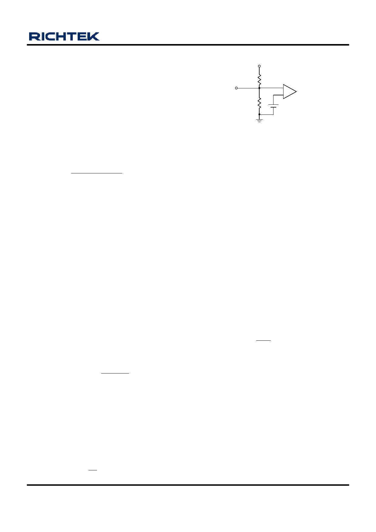
Setting the Output voltage
The output voltage is set by external voltage divider and
reference voltage. The feedback pin (FB, LFB1, and LFB2)
is connected to the inverting input of error amplifier and is
referenced to 0.8V reference voltage at non-inverting input
as shown in Figure 3.The output voltage is set by the
following equation.
Ra
VOUT = (1+ ) × 0.8
(12)
Rb
DS9206-11 March 2007
VOUT
FB
(LFB1,LFB2)
Ra
Rb
-
+
0.8V
Figure 3. The connected diagram of external voltage
divider and reference voltage
If high value resistors are used, the input bias current of
FB pin could cause a slight increase in output voltage.
The output voltage set point can be more accurate by using
precision resistor.
Soft-start setting
Figure 4 shows the typical soft-start timing waveforms of
RT9206. The soft-start time of Buck converter can be set
by selecting the soft-start capacitance value. The delay
time between input voltage applied and output voltage
starting to ramp up (TDELAY) is calculated as: The total
time from input voltage applied to output voltage buildup
(TVR) is calculated as :
TVR = 57 × CSS ×106
(ms) (13)
The effective soft-start time (TSS) during that output voltage
ramps up from zero to set voltage is calculated as :
TSS = (320 × VOUT ) ×106 × CSS
VIN
(ms) (14)
Besides, appropriate soft-start capacitor should be selected
so that the start-up current will not trigger the current limit
function. And make sure that the input power source could
supply the soft-start current.
The total time from input voltage applied to power good
signal pull-high (TPGOOD) is calculated as :
TPG = 640 × CSS ×106
(ms) (15)
www.richtek.com
15
Share Link: 