RT9206 Ver la hoja de datos (PDF) - Richtek Technology
Número de pieza
componentes Descripción
Fabricante
RT9206 Datasheet PDF : 21 Pages
| |||
RT9206
VDD
VSS
VOUT
TVR
PGOOD
TSS
TPGOOD
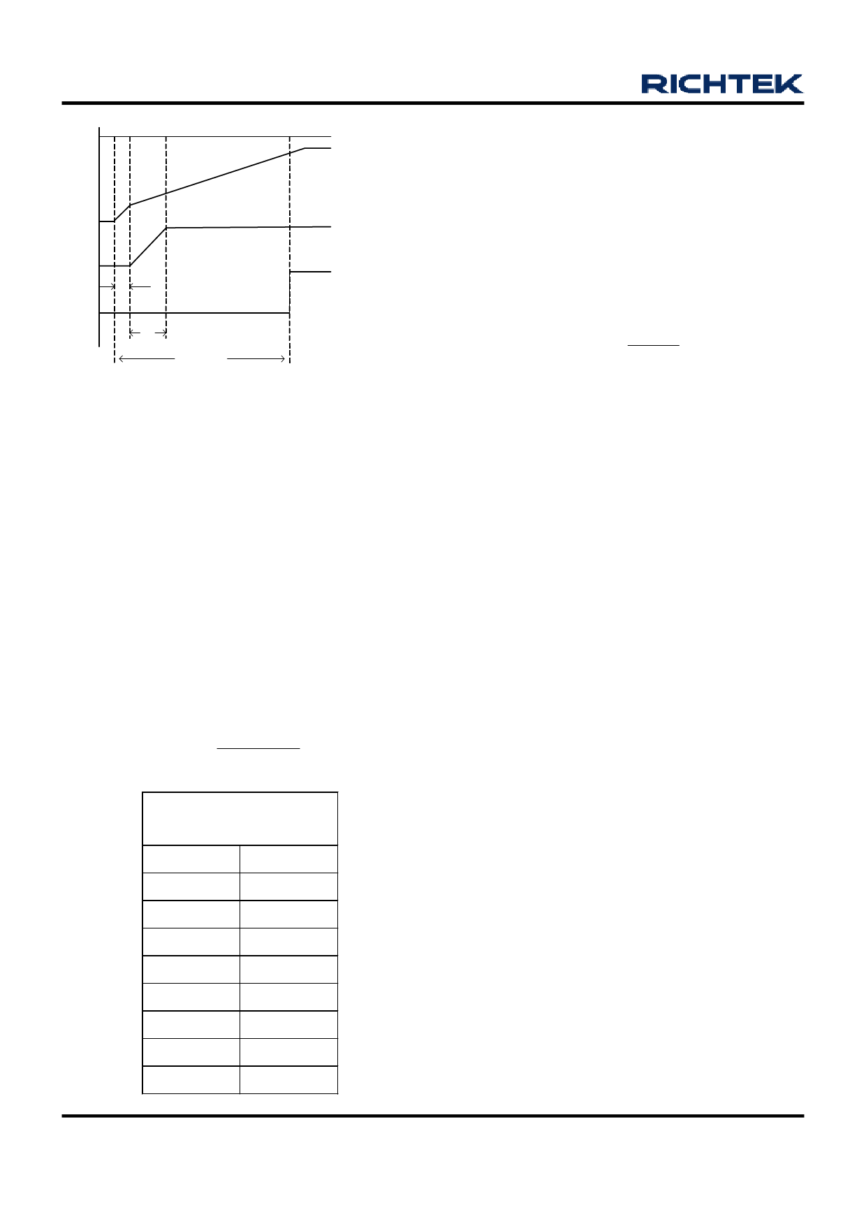
Figure 4. The soft-stat timing diagram of RT9206
For the example of CSS = 1µF, VIN = 12V, VOUT = 5V, then
TVR = 57ms, TSS = 133ms and TPGOOD = 640ms.
Shutdown
The power stage can be shutdown by pulling soft-start pin
below 0.7V. During shutdown, both of high side MOSFET
(S1) and low side MOSFET (S2) are turned off.
Setting the switching frequency
The switching frequency can be set by a resistor (RRT)
connecting between RT and GND pins. Equation (16)
describes the relationship of RRT and switching frequency.
As RT open the normally operated frequency is 200kHz.
62 ×108
RRT =
fS - 200 ×103
(Ω)
(16)
RRT Connecting Between
RT and GND Pins
fS(kHz)
250
RRT (kΩ)
120
300
55
350
37.5
400
30.6
450
24.4
500
22.5
550
19.3
600
16.8
Boost Component Selection
The booststrap gate drive circuit is used to drive high side
N-channel MOSFET. The boost capacitor should be a good
quality and can operate in high frequency. The value of
boost capacitor depends on the total gate charge (QHg) to
turn on the MOSFETs. Assuming steady state operation,
the following equation can be used to calculate the
capacitance value to achieve the targeted ripple voltage
∆VBOOT .
QHg
CBOOT =
(F)
ΔVBOOT
The capacitor in the range of 0.1uF to 1uF is generally
adequate for most applications.
The VINT pin bypass capacitor CINT needs to charge the
boost capacitor, to drive the low side MOSFET, and to power
the RT9206. CINT should locate near VINT and GND pins
with short and wide traces. Generally, a 4.7uF high
frequency ceramic capacitor is recommended.
Feedback Compensation
The RT9206 is a voltage mode controller. The control loop
is a single voltage feedback loop including a trans-
conductance error amplifier and a PWM comparator.
To achieve fast transient response and accurate output
regulation, appropriate feedback compensation is
necessary. The goal of the compensation network is to
provide a closed loop transfer function with the highest
0dB crossing frequency and adequate phase margin.
Generally, the phase margin in a range of 45° ~ 60° is
desirable. Figure 4 shows the simplified diagram of
synchronous buck converter and control loop.
www.richtek.com
16
DS9206-11 March 2007
Share Link: 