NCP3020A Ver la hoja de datos (PDF) - ON Semiconductor
Número de pieza
componentes Descripción
Fabricante
NCP3020A Datasheet PDF : 23 Pages
| |||
NCP3020A, NCP3020B, NCV3020A, NCV3020B
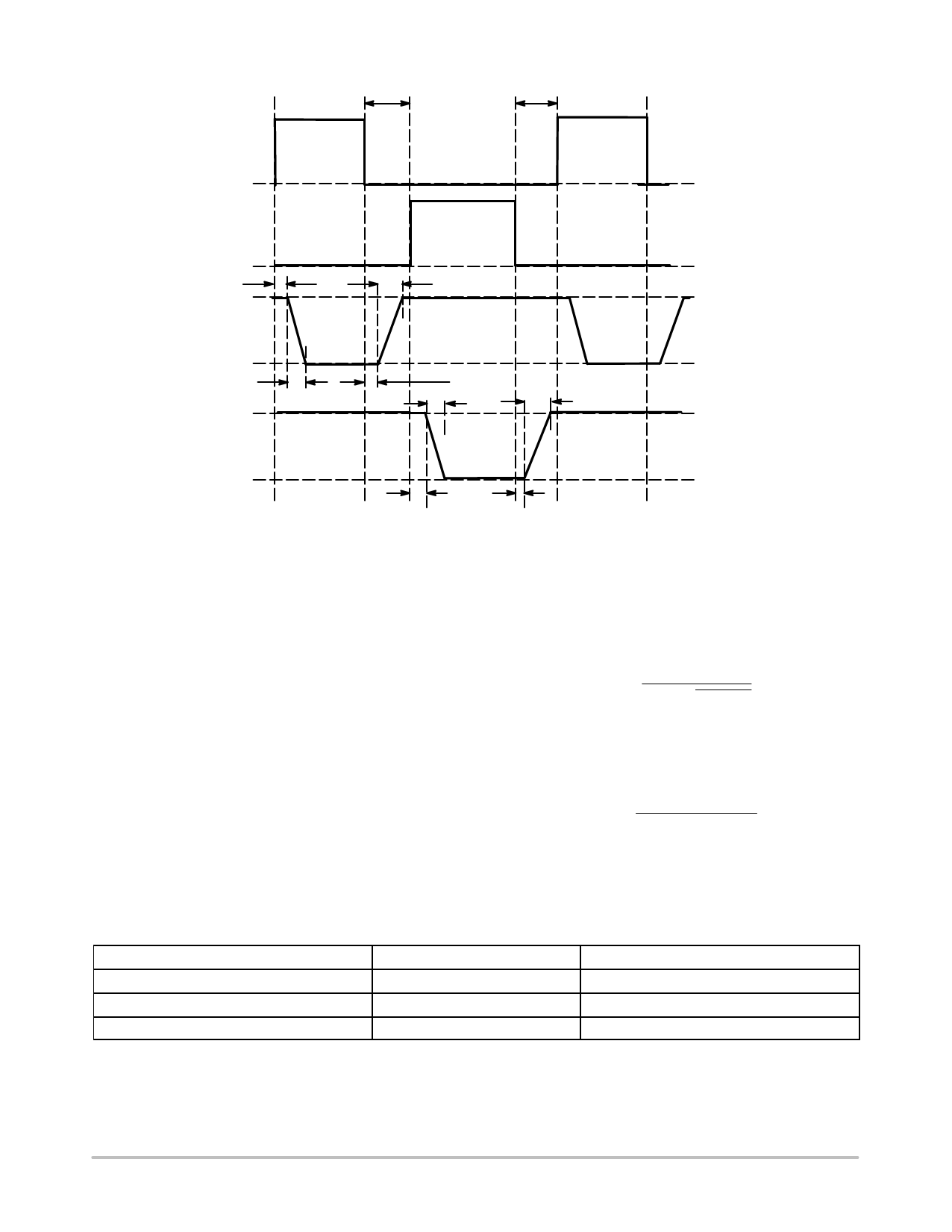
NOLHL
NOLLH
High−Side
Logic Signal
Low−Side
Logic Signal
RDSmax
High−Side
MOSFET
RDS(on)min
RDSmax
Low−Side
MOSFET
RDS(on)min
td(on)
tf
tr
td(off)
tr
tf
td(on)
td(off)
Figure 34. MOSFETs Timing Diagram
Another consideration during MOSFET selection is their
delay times. Turn−on and turn−off times must be short
enough to prevent cross conduction. If not, there will be
conduction from the input through both MOSFETs to
ground. Therefore, the following conditions must be met.
td(ON)_CONTROL ) NOLLH u td(OFF)_SYNC ) t f_SYNC
and
(eq. 37)
t(ON)_SYNC ) NOLHL u td(OFF)_CONTROL ) t f _CONTROL
The MOSFET parameters, td(ON), tr, td(OFF) and tf are can
be found in their appropriate datasheets for specific
conditions. NOLLH and NOLHL are the dead times which
were described earlier and are 85 ns and 75 ns, respectively.
Feedback and Compensation
The NCP3020 is a voltage mode buck convertor with a
transconductance error amplifier compensated by an
external compensation network. Compensation is needed to
achieve accurate output voltage regulation and fast transient
response. The goal of the compensation circuit is to provide
a loop gain function with the highest crossing frequency and
adequate phase margin (minimally 45°). The transfer
function of the power stage (the output LC filter) is a double
pole system. The resonance frequency of this filter is
expressed as follows:
fP0
+
2
@
p
@
1
ǸL
@
COUT
(eq. 38)
Parasitic Equivalent Series Resistance (ESR) of the
output filter capacitor introduces a high frequency zero to
the filter network. Its value can be calculated by using the
following equation:
fZ0
+
2
@
p
@
1
COUT
@
ESR
(eq. 39)
The main loop zero crossover frequency f0 can be chosen
to be 1/10 − 1/5 of the switching frequency. Table 2 shows
the three methods of compensation.
Table 2. COMPENSATION TYPES
Zero Crossover Frequency Condition
fP0 < fZ0 < f0 < fS/2
fP0 < f0 < fZ0 < fS/2
fP0 < f0 < fS/2 < fZ0
Compensation Type
Type II
Type III Method I
Type III Method II
Typical Output Capacitor Type
Electrolytic, Tantalum
Tantalum, Ceramic
Ceramic
http://onsemi.com
20
Share Link: 