NCP3020A Ver la hoja de datos (PDF) - ON Semiconductor
Número de pieza
componentes Descripción
Fabricante
NCP3020A Datasheet PDF : 23 Pages
| |||
NCP3020A, NCP3020B, NCV3020A, NCV3020B
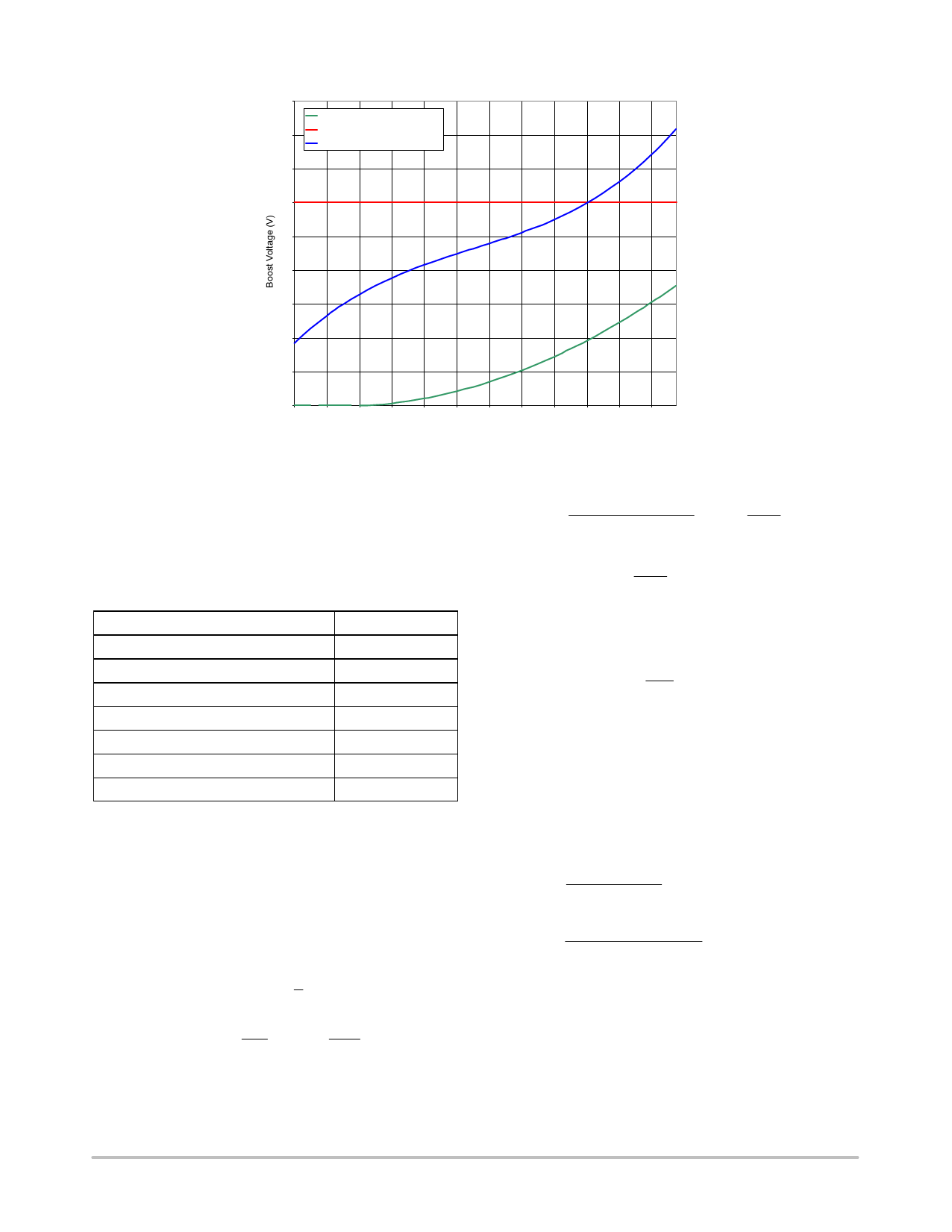
Boost Voltage
18
Voltage Ripple
16
Maximum Allowable Voltage
Maximum Boost Voltage
14
12
10
8
6
4
2
0
4.5 6.5 8.5 10.5 12.5 14.5 16.5 18.5 20.5 22.5 24.5 26.5
Input Voltage (V)
Figure 31. Boost Voltage at 80% Duty Cycle
Inductor Selection
When selecting the inductor, it is important to know the
input and output requirements. Some example conditions
are listed below to assist in the process.
Table 1. DESIGN PARAMETERS
Design Parameter
Input Voltage
Nominal Input Voltage
Output Voltage
Input ripple voltage
Output ripple voltage
Output current rating
Operating frequency
(VIN)
(VIN)
(VOUT)
(VINRIPPLE)
(VOUTRIPPLE)
(IOUT)
(Fsw)
Example Value
9 V to 18 V
12 V
3.3 V
300 mV
50 mV
10 A
300 kHz
A buck converter produces input voltage (VIN) pulses that
are LC filtered to produce a lower dc output voltage (VOUT).
The output voltage can be changed by modifying the on time
relative to the switching period (T) or switching frequency.
The ratio of high side switch on time to the switching period
is called duty cycle (D). Duty cycle can also be calculated
using VOUT, VIN, the low side switch voltage drop VLSD,
and the High side switch voltage drop VHSD.
F+1
T
(eq. 3)
D + TON (* D Ǔ + TOFF
T
T
(eq. 4)
D+
VOUT ) VLSD
[ D + VOUT
VIN * VHSD ) VLSD
VIN
(eq. 5)
3.3 V
³ 27.5% +
12 V
The ratio of ripple current to maximum output current
simplifies the equations used for inductor selection. The
formula for this is given in Equation 6.
ra + DI
IOUT
(eq. 6)
The designer should employ a rule of thumb where the
percentage of ripple current in the inductor lies between
10% and 40%. When using ceramic output capacitors the
ripple current can be greater thus a user might select a higher
ripple current, but when using electrolytic capacitors a lower
ripple current will result in lower output ripple. Now,
acceptable values of inductance for a design can be
calculated using Equation 7.
L+
VOUT
@ (1 * D) ³ 3.3 mH
IOUT @ ra @ FSW
3.3 V
+
@ (1 * 27.5%)
10 A @ 24% @ 300 kHz
(eq. 7)
The relationship between ra and L for this design example
is shown in Figure 32.
http://onsemi.com
16
Share Link: 