LTC4218CGN(RevB) Ver la hoja de datos (PDF) - Linear Technology
Número de pieza
componentes Descripción
Fabricante
LTC4218CGN Datasheet PDF : 16 Pages
| |||
LTC4218
APPLICATIONS INFORMATION
its threshold. The PG then pulls low to indicate output
power is no longer good.
If VDD drops below 2.65V for greater than 5μs or INTVCC
drops below 2.5V for greater than 1μs, a fast shutdown
of the switch is initiated. The GATE is pulled down with a
170mA current to the SOURCE pin.
Overcurrent Fault
The LTC4218 features an adjustable current limit with
foldback that protects the MOSFET when excessive load
current happens. To protect the switch during active cur-
rent limit, the available current is reduced as a function
of the output voltage sensed by the FB pin. A graph in the
Typical Performance Characteristics shows the current
limit versus FB voltage.
An overcurrent fault occurs when the current limit circuitry
has been engaged for longer than the time-out delay set by
the TIMER. Current limiting begins when the current sense
voltage between the SENSE+ and SENSE– pins reaches
3.75mV to 15mV (depending on the foldback). The GATE
pin is then brought down with a 170mA GATE-to-SOURCE
current. The voltage on the GATE is regulated in order to
limit the current sense voltage to less than 15mV. At this
point, a circuit breaker time delay starts by charging the
external timing capacitor from the TIMER pin with a 100μA
pull-up current. If the TIMER pin reaches its 1.2V thresh-
old, the external switch turns off (with a 250μA current
from GATE to ground). Next, the FLT pin is pulled low to
indicate an overcurrent fault has turned off the MOSFET.
For a given the circuit breaker time delay, the equation for
setting the timing capacitor’s value is as follows:
CT = TCB • 0.083[μF/ms]
After the switch is turned off, the TIMER pin begins dis-
charging the timing capacitor with a 2μA pull-down current.
When the TIMER pin reaches its 0.2V threshold, the switch
is allowed to turn on again if the overcurrent fault has been
cleared. Bringing the UV pin below 0.6V and then high will
clear the fault. If the TIMER pin is tied to INTVCC, then the
switch is allowed to turn on again (after an internal 100ms
delay) if the overcurrent fault is cleared.
Tying the FLT pin to the UV pin allows the part to self-clear
the fault and turn the MOSFET on as soon as TIMER pin has
ramped below 0.2V. In this auto retry mode, the LTC4218
repeatedly tries to turn on after an overcurrent at a period
determined by the capacitor on the TIMER pin.
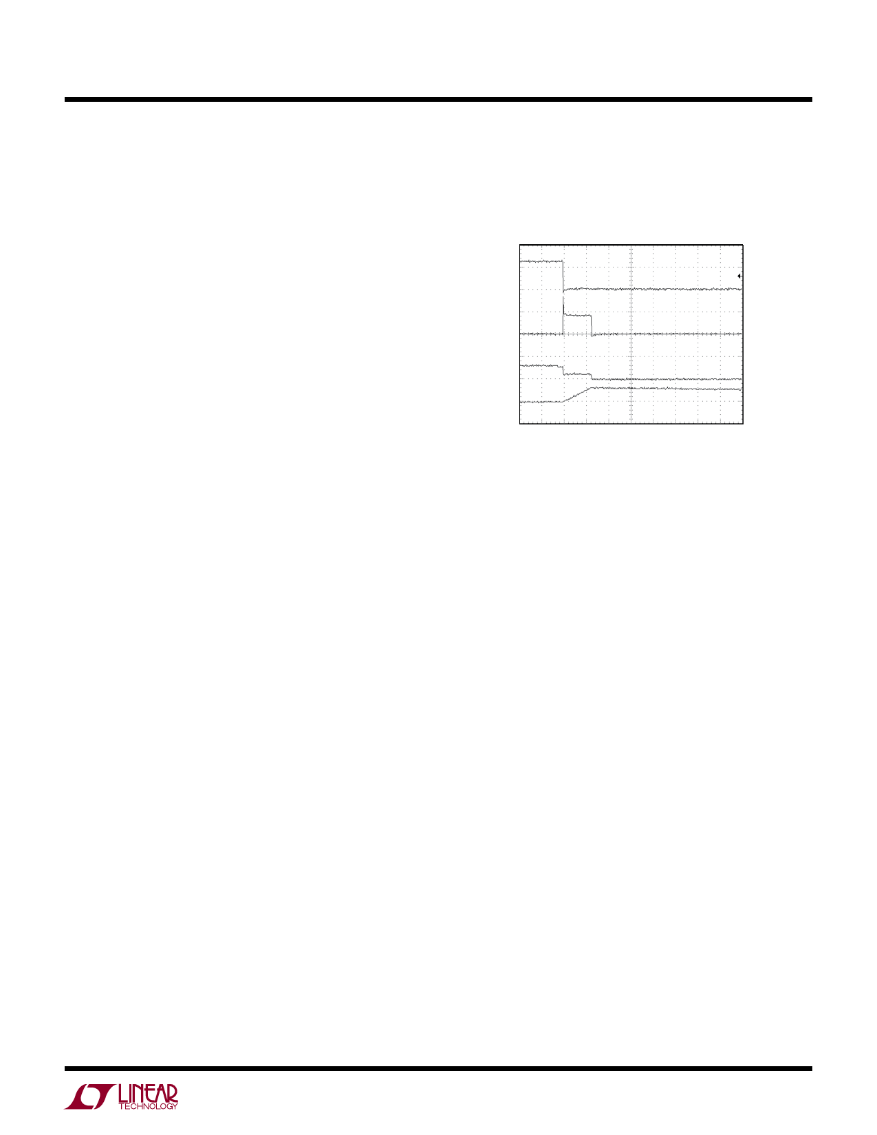
The waveform in Figure 3 shows how the output latches
off following a short circuit. The drop across the sense
resistor is 3.75mV as the timer ramps up.
VOUT
10V/DIV
IOUT
2A/DIV
ΔVGATE
10V/DIV
TIMER
2V/DIV
1ms/DIV
4218 F03
Figure 3. Short-Circuit Waveform
Current Limit Adjustment
The default value of the active current limiting signal
threshold is 15mV. The current limit threshold can be
adjusted lower by placing a resistor on the ISET pin. As
shown in the Functional Diagram the voltage at the ISET
pin (via the clamp circuit) sets the CS amplifier’s built-in
offset voltage. This offset voltage directly determines the
active current limit value. With the ISET pin open, the volt-
age at the ISET pin is determined by the buffered reference
voltage. This voltage is set to 0.618V which corresponds
to a 15mV current limit threshold.
An external resistor placed between the ISET pin and ground
forms a resistive divider with the internal 20k sourcing
resistor. The divider acts to lower the voltage at the ISET
pin and therefore lower the current limit threshold. The
overall current limit threshold precision is reduced to ±11%
when using a 20k resistor to half the threshold.
4218fb
11
Share Link: 