E28F004BL-T150 Ver la hoja de datos (PDF) - Intel
Número de pieza
componentes Descripción
Fabricante
E28F004BL-T150 Datasheet PDF : 44 Pages
| |||
28F400BL-T B 28F004BL-T B
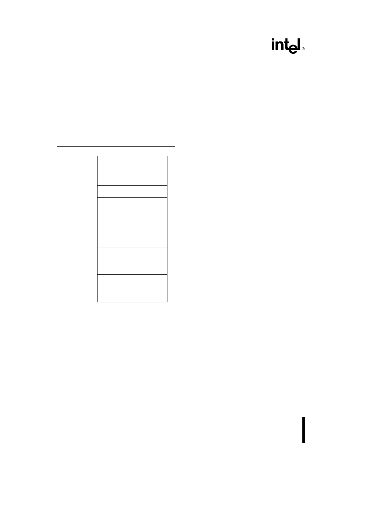
3 1 2 2 28F004BL-T Memory Map
The 28F004BL-T device has the 16-Kbyte boot
block located from 7C000H to 7FFFFH to accom-
modate those microprocessors that boot from the
top of the address map In the 28F004BL-T the first
8-Kbyte parameter block resides in memory space
from 7A000H to 7BFFFH The second 8-Kbyte pa-
rameter block resides in memory space from
78000H to 79FFFH The 96-Kbyte main block re-
sides in memory space from 60000H to 77FFFH
The three 128-Kbyte main blocks reside in memory
space from 40000H to 5FFFFH 20000H to 3FFFFH
and 00000H to 1FFFFH
7FFFFH
7C000H
7BFFFH
7A000H
79FFFH
78000H
77FFFH
60000H
5FFFFH
40000H
3FFFFH
20000H
1FFFFH
16-Kbyte BOOT BLOCK
8-Kbyte PARAMETER BLOCK
8-Kbyte PARAMETER BLOCK
96-Kbyte MAIN BLOCK
128-Kbyte MAIN BLOCK
128-Kbyte MAIN BLOCK
128-Kbyte MAIN BLOCK
00000H
Figure 11 28F004BL-T Memory Map
4 0 PRODUCT FAMILY PRINCIPLES
OF OPERATION
Flash memory augments EPROM functionality with
in-circuit electrical write and erase The 4-Mbit flash
memory family utilizes a Command User Interface
(CUI) and internally generated and timed algorithms
to simplify write and erase operations
The CUI allows for fixed power supplies during era-
sure and programming and maximum EPROM com-
patibility
In the absence of high voltage on the VPP pin the
4-Mbit flash family will only successfully execute the
following commands Read Array Read Status Reg-
ister Clear Status Register and Intelligent Identifier
mode The device provides standard EPROM read
standby and output disable operations Manufactur-
er Identification and Device Identification data can
be accessed through the CUI or through the stan-
dard EPROM A9 high voltage access (VID) (for
PROM programmer equipment)
The same EPROM read standby and output disable
functions are available when high voltage is applied
to the VPP pin In addition high voltage on VPP al-
lows write and erase of the device All functions as-
sociated with altering memory contents write and
erase Intelligent Identifier read and Read Status are
accessed via the CUI
The purpose of the Write State Machine (WSM) is to
completely automate the write and erasure of the
device The WSM will begin operation upon receipt
of a signal from the CUI and will report status back
through a Status Register The CUI will handle the
WE interface to the data and address latches as
well as system software requests for status while the
WSM is in operation
4 1 28F400BL Bus Operations
Flash memory reads erases and writes in-system
via the local CPU All bus cycles to or from the flash
memory conform to standard microprocessor bus
cycles
16
Share Link: 