L1N08LE Ver la hoja de datos (PDF) - Intersil
Número de pieza
componentes Descripción
Fabricante
L1N08LE Datasheet PDF : 9 Pages
| |||
RLP1N08LE
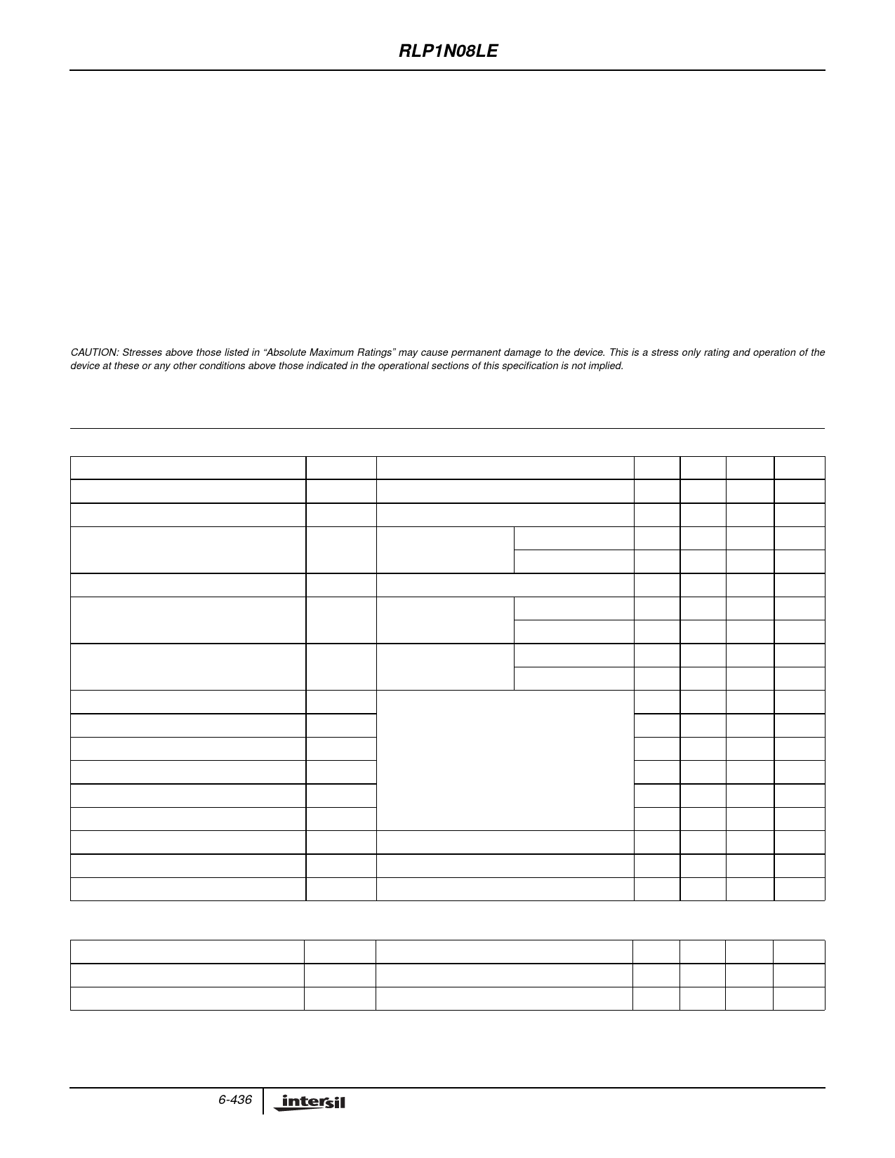
Absolute Maximum Ratings TC = 25oC, Unless Otherwise Specified
Drain to Source Voltage (Note 1) . . . . . . . . . . . . . . . . . . . . . . . . . . . . . . . . . . . . . . . . . . . . . VDSS
Drain to Gate Voltage (RGS = 20kΩ) (Note 1) . . . . . . . . . . . . . . . . . . . . . . . . . . . . . . . . . . .VDGR
Electrostatic Voltage at 100pF, 1500Ω . . . . . . . . . . . . . . . . . . . . . . . . . . . . . . . . . . . . . . . . . .ESD
Continuous Drain Current . . . . . . . . . . . . . . . . . . . . . . . . . . . . . . . . . . . . . . . . . . . . . . . . . . . . .ID
Gate to Source Voltage (Reverse Voltage Gate Bias Not Allowed) . . . . . . . . . . . . . . . . . . . . VGS
Maximum Power Dissipation . . . . . . . . . . . . . . . . . . . . . . . . . . . . . . . . . . . . . . . . . . . . . . . . . . PD
Power Dissipation Derating . . . . . . . . . . . . . . . . . . . . . . . . . . . . . . . . . . . . . . . . . . . . . . . . . . . . .
Operating and Storage Temperature . . . . . . . . . . . . . . . . . . . . . . . . . . . . . . . . . . . . . . . TJ, TSTG
Maximum Temperature for Soldering
Leads at 0.063in (1.6mm) from Case for 10s. . . . . . . . . . . . . . . . . . . . . . . . . . . . . . . . . . . . TL
Package Body for 10s, See Techbrief 334 . . . . . . . . . . . . . . . . . . . . . . . . . . . . . . . . . . . . .Tpkg
RLP1N08LE
80
80
2
Self Limited
5.5
30
0.24
-55 to 150
300
260
UNITS
V
V
kV
V
W
W/oC
oC
oC
oC
CAUTION: Stresses above those listed in “Absolute Maximum Ratings” may cause permanent damage to the device. This is a stress only rating and operation of the
device at these or any other conditions above those indicated in the operational sections of this specification is not implied.
NOTE:
1. TJ = 25oC to 150oC.
Electrical Specifications TC = 25oC, Unless Otherwise Specified
PARAMETER
SYMBOL
TEST CONDITIONS
Drain to Source Breakdown Voltage
Gate to Threshold Voltage
Zero Gate Voltage Drain Current
Gate to Source Leakage Current
Drain to Source On Resistance (Note 2)
Limiting Current
Turn-On Time
Turn-On Delay Time
Rise Time
Turn-Off Delay Time
Fall Time
Turn-Off Time
Thermal Resistance Junction to Case
Thermal Resistance Junction to Ambient
Electrostatic Voltage
BVDSS
VGS(TH)
IDSS
IGSS
rDS(ON)
IDS(Lim)
t(ON)
td(ON)
tr
td(OFF)
tf
t(OFF)
RθJC
RθJA
ESD
ID = 250µA, VGS = 0V, Figure 7
VGS = VDS, ID = 250µA, Figure 8
VDS = 65V, VGS = 0V TC = 25oC
TC = 150oC
VGS = 5V, TC = 150oC
ID = 1A, VGS = 5V
Figure 6
TC = 25oC
TC = 150oC
VDS = 15V, VGS = 5V
Figure 3
TC = 25oC
TC = 150oC
VDD = 30V, ID = 1A, VGS = 5V, RGS = 25Ω
RL = 30Ω
TO-220AB
Human Model (100pF, 1.5kΩ)
MIN
80
1
-
-
-
-
-
1.8
1.1
-
-
1
-
1
-
-
-
2000
TYP
-
-
-
-
-
-
-
-
-
-
-
-
-
-
-
-
-
-
MAX
-
2
1
50
50
0.750
1.5
3
1.5
6.5
1.5
5
7.5
5
12.5
4.17
62
-
UNITS
V
V
µA
µA
µA
Ω
Ω
A
A
µs
µs
µs
µs
µs
µs
oC/W
oC/W
V
Source to Drain Diode Specifications
PARAMETER
SYMBOL
TEST CONDITIONS
Source to Drain Diode Voltage (Note 2)
VSD
ISD = 1A
Reverse Recovery Time
trr
ISD = 1A
NOTES:
2. Pulsed: pulse duration = ≤ 300µs maximum, duty cycle = ≤ 2%.
3. Repititive rating: pulse width limited by maximum junction temperature.
MIN TYP MAX UNITS
-
-
1.5
V
-
-
1
ms
6-436
Share Link: 