UT1750AR12WCC Ver la hoja de datos (PDF) - Aeroflex UTMC
Número de pieza
componentes Descripción
Fabricante
UT1750AR12WCC Datasheet PDF : 56 Pages
| |||
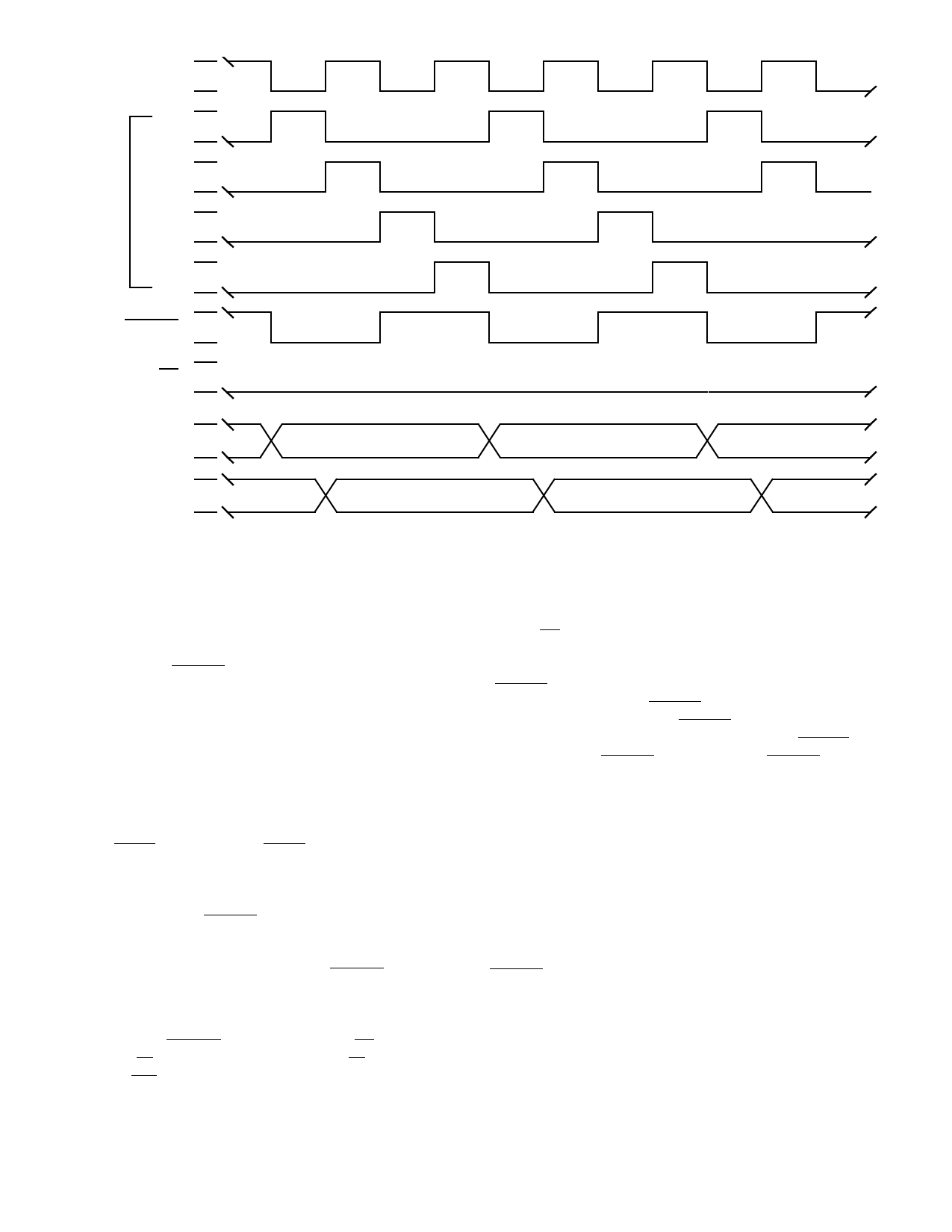
OSCIN
CK1
CK2
CK3
CK4
STATE1
OE
INSTRUCTION
ADDRESS
VALID ADDRESS
VALID ADDRESS
INSTRUCTION
DATA
VALID DATA
VALID DATA
Figure 25b. Typical UT1750AR Bus Cycle
During the time period CK1, the UT1750AR begins executing
the instruction in the Primary Instruction Register (PIR). The
instruction executed is the instruction the UT1750AR fetched
during the previous bus cycle, thus the overlapping fetch and
execute cycles of the UT1750AR. During CK1, the RISC
address for the next instruction to fetch from memory becomes
valid. Also, the STATE1 output goes low, indicating the
UT1750AR is executing an instruction.
At the beginning of time period CK2, the data addressed during
CK1 becomes valid. The following conditions extend time
period CK2 one clock cycle: (1) Executing a STRI instruction,
(2) Executing a LRI instruction, or (3) Executing any instruction
with Long Immediate data. The UT1750AR also extends clock
period CK2 because of the Operand bus arbitration process. The
UT1750AR samples the logical AND combination of the Bus
Busy (BUSY) and Bus Grant (BGNT) inverted on the falling
edge of CK2. If this combination is low during the falling edge
of CK2, time period CK2 extends until the combination of the
two signals is high, indicating the UT1750AR now controls the
Operand busses. The STATE1 output remains low for the entire
CK2 time period.
At the beginning of time period CK3, the STATE1 output goes
high indicating the next instruction is being fetched from
memory. The UT1750AR’s Operand address and data busses
become active at the beginning of CK3 along with the Bus Grant
Acknowledge (BGACK), the Address Strobe (AS), the Memory
or I/O (M/IO), the Operand/ Instruction (OP/IN), and the Read/
Write (R/WR) signals.
After time period CK4 starts, the transparent latches that make
up the Primary Instruction Register open up allowing the
UT1750AR to input the instruction from RISC memory. Since
the instruction being executed requires Operand data, the Data
Strobe (DS) goes active on the falling edge of the processor
clock, one-half clock period after the rising edge of CK4. The
UT1750AR now samples the Data Transfer Acknowledge
(DTACK) signal on the next and every subsequent rising edge
of the processor clock. If DTACK is not low, the UT1750AR
extends time period CK4 until DTACK becomes active or until
an error condition is detected -- either Bus Error (BTERR) or
Memory Protect (MPROT) becomes active. STATE1 remains
high during the entire CK4 time period.
The Processor bus cycle just described is for an instruction that
requires some type of Operand data. Figure 25b shows a
UT1750AR bus cycle when no Operand data is required. This
cycle is typical of the bus cycle occurring for instructions that
only require internal processing. An example of this type of
instruction is a Move Register-to-Register instruction. For this
type of instruction, each instruction requires two processor clock
cycles for execution. Neither time period (CK2 nor CK4) is
extended because of Operand bus arbitration or a delayed
DTACK.
22
Share Link: 