UT1750AR12WCC Ver la hoja de datos (PDF) - Aeroflex UTMC
Número de pieza
componentes Descripción
Fabricante
UT1750AR12WCC Datasheet PDF : 56 Pages
| |||
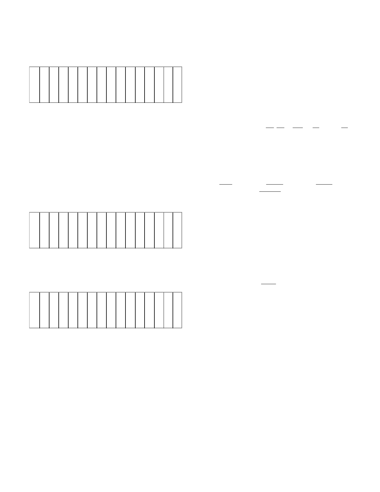
Program Counter Register (PC)
The Program Counter Register (PC) (figure 23) contains the 16-
bit address for the present MIL-STD-1750A instruction. The
RISC I/O instruction reads from or writes to the PC.
15 14 13 12 11 10 9 8 7 6 5 4 3 2 1 0
P P PPPPP PPP PPPPPP
C C CCCCC CCC CCCCCC
1 1 11119 876 54 3210
5 43210
MSB
LSB
Figure 23. The Program Counter Register (PC)
1750 Timer A (TA) and 1750 Timer B (TB)
The Timer A (TA) and Timer B (TB) registers, figures 24a and
24b respectively, are 16-bit binary counters as defined by MIL-
STD-1750A. The RISC I/O instruction starts, halts, reads, and
loads them. When one of the timers reaches its programmed
time setting, such as going from FFFFH to 0000H, a timeout
occurs. This timeout sets the appropriate bit in the Pending
Interrupt Register (PI).
15 14 13 12 11 10 9 8 7 6 5 4 3 2 1 0
T T TTTTT TTT TTTTTT
A A AAAAA AAA AAAAAA
1 1 11119 876 54 3210
5 43210
MSB
LSB
Figure 24a. 1750 Timer A (TA)
15 14 13 12 11 10 9 8 7 6 5 4 3 2 1 0
T T TTTTT TTT TTTTTT
B B BBBBB BBB BBBBBB
1 1 11119 876 54 3210
5 43210
MSB
Figure 24b. 1750 Timer B (TB)
LSB
SYSTEM INTERFACE
The System Interface describes how the Instruction and
Operand address and data busses operate during the
UT1750AR’s many machine cycles and bus operations. The
discussion about the UT1750AR’s machine cycles and bus
operations applies to both the RISC mode and the MIL-STD-
1750A mode of operation, since in the 1750 mode of operation
the UT1750AR executes a specialized set of RISC macros that
allow the UT1750AR to emulate the MIL-STD-1750A
Instruction Set Architecture.
The UT1750AR has the following seven types of machine
operations or bus cycle operations:
• Data Bus Cycle Operation
• DMA Operation and Bus Arbitration
• Interrupt Operation and Exception Handling
• RISC Instruction Bus Cycle Operation
• Internal UART Operation
• Console Mode of Operation
• 1750 Instruction Memory Mapping
Operand Bus and Instruction Bus Interfaces
The UT1750AR Operand Data Bus interface supports multiple
processor and Direct Memory Access (DMA) configurations.
The Operand Address Bus (A15-A0), Data Bus (D15-D0), and
memory control bus signals (AS, DS, R/WR, M/IO, and OP/IN)
are TTL-compatible signals that may be placed in a high-
impedance state. These signals are only active during bus cycles
when the UT1750AR is the current bus master. On other bus
cycles, these signals enter a high-impedance state so an alternate
bus master can control the busses.
The four signals that make up the Arbitration Control Bus -- Bus
Request (BRQ), Bus Grant (BGNT), Bus Busy (BUSY), and
Bus Grant Acknowledge (BGACK) -- control the UT1750AR’s
Operand Data Bus arbitration process. The arbitration process
allows asynchronous bus arbitration.
The Instruction Bus does not allow any type of bus arbitration.
The UT1750AR is the only device permitted to access
Instruction memory; this access is generally confined to reading
RISC instructions the UT1750AR subsequently executes,
although the RISC instruction set does provide one instruction
the UT1750AR uses to alter RISC memory. This instruction is
the Store Register to Instruction Memory (STRI).
The Instruction address and data busses only enter a high-
impedance state when the TEST input is low.
A TYPICAL UT1750AR BUS CYCLE
Figure 25a (see page 21), a generalized diagram for a typical
UT1750AR bus cycle, shows the UT1750AR’s bus cycle
separated into four distinct time periods (CK1 through CK4).
These time periods are based on the processor clock. The
UT1750AR performs a separate function during each of these
four time periods.
20
Share Link: 