M80C186 Ver la hoja de datos (PDF) - Intel
Número de pieza
componentes Descripción
Fabricante
M80C186 Datasheet PDF : 59 Pages
| |||
M80C186
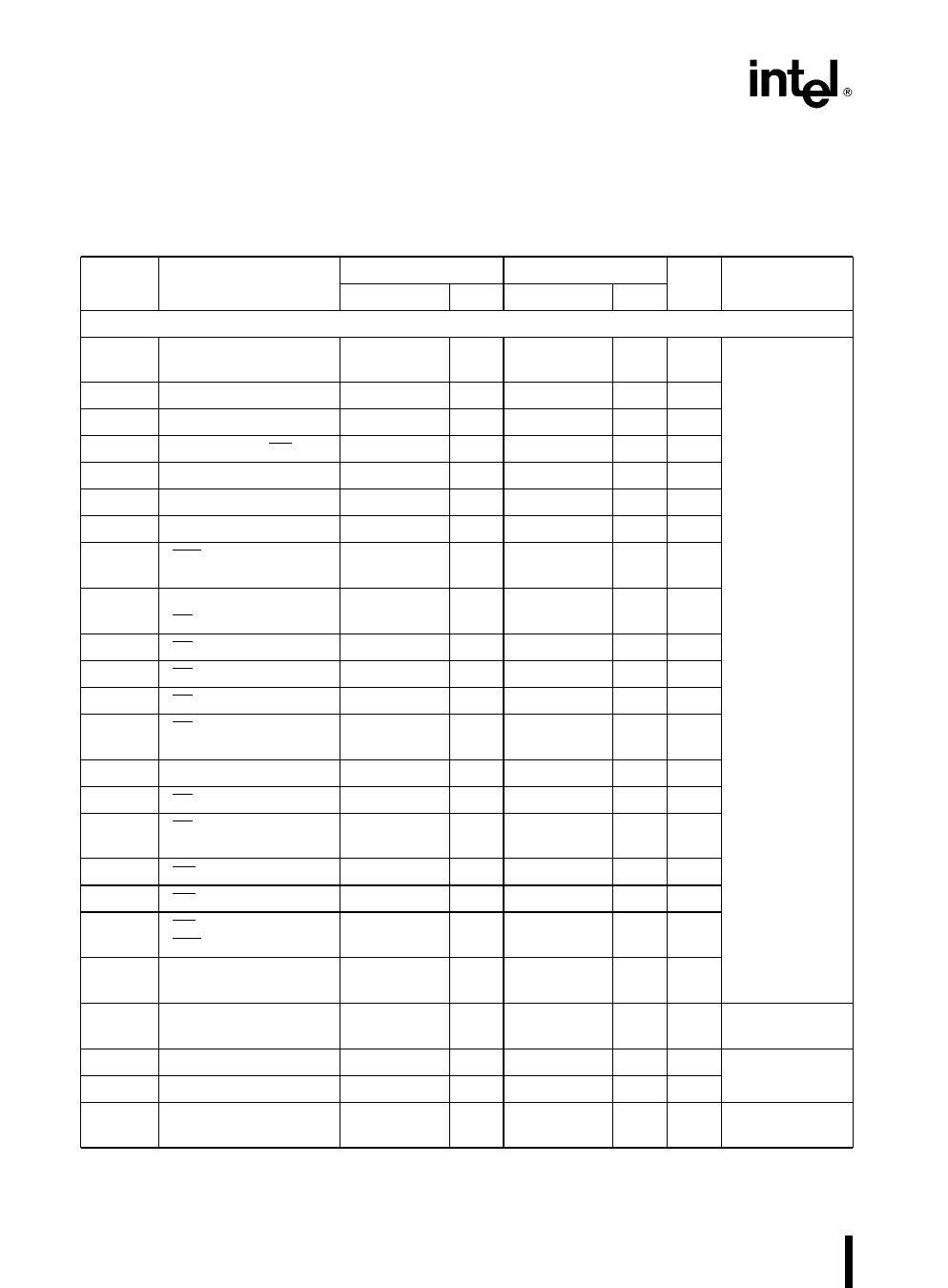
PIN TIMINGS (Continued)
AC CHARACTERISTICS (Over Specified Operating Conditions) (Continued)
All timings are measured at 1 5V and 100 pF loading on CLKOUT unless otherwise noted
All output test conditions are with CL e 50 – 200 pF (10 MHz) and CL e 50 – 100 pF (12 5 MHz)
For AC tests input VIL e 0 45V and VIN e 2 4V except at X1 where VIH e VCC b 0 5V
Symbol
Parameter
M80C186-10
Min
Max
M80C186-12
Unit
Min
Max
Comments
M80C186 MASTER INTERFACE TIMING RESPONSES (Continued)
TLLAX
Address Hold to
TCHCL b 20
TCHCL 15
ns
ALE Inactive (min)
TCLDV
Data Valid Delay
5
40
5
36
TCLDOX Data Hold Time
3
3
TWHDX
Data Hold after WR (min) TCLCL b 34
TCLCL b 20
TCVCTV Control Active Delay 1
3
56
3
47
TCHCTV Control Active Delay 2
5
44
5
37
TCVCTX Control Inactive Delay
4
44
5
37
TCVDEX
DEN Inactive Delay
(Non-Write Cycle)
5
56
5
47
TAZRL
Address Float to
0
0
RD Active
TCLRL
RD Active Delay
5
44
5
37
TCLRH
RD Inactive Delay
5
44
5
37
tRHLH
RD Inactive to ALE High TCLCH b 14
TCLCH b 14
TRHAV
RD Inactive to
Address Active (min)
TCLCL b 40
TCLCL b 20
TCLHAV
TRLRH
TRVCH
HLDA Valid Delay
RD Pulse Width (min)
RD Valid to
Clock High
5
40
4
33
2TCLCL b 46
25
2TCLCL b 40
25
ns
ns
ns
ns
ns
ns
ns
CL e
ns
50 pF – 200 pF b
all outputs
(except TCLTMV)
ns
10 MHz
ns
ns
CL e
ns 50 pF – 100 pF
all outputs
12 5 MHz
ns
ns
ns
TWLWH WR Pulse Width (min)
2TCLCL b 34
2TCLCL b 30
ns
tWHLH
WR Inactive to AEE High TCLCH b 14
TCLCH b 14
ns
TWHDEX
WR Inactive to
DEN Inactive
TCLCH b 10
TCLCH b 10
ns
TCSVLL
Chip Select Valid
TCLCH b 14
TCLCH b 14
ns
to ALE Low
TAVLL
Address Valid to
TCLCH b 19
TCLCH b 15
ns
ALE Low (min)
TCHSV
TCLSH
TCLTMV
Status Active Delay
Status Inactive Delay
Timer Output Delay
5
45
5
35
ns
5
50
5
35
ns
48
40
ns 100 pF max
10 MHz
46
Share Link: 