M80C186 Ver la hoja de datos (PDF) - Intel
Número de pieza
componentes Descripción
Fabricante
M80C186 Datasheet PDF : 59 Pages
| |||
M80C186
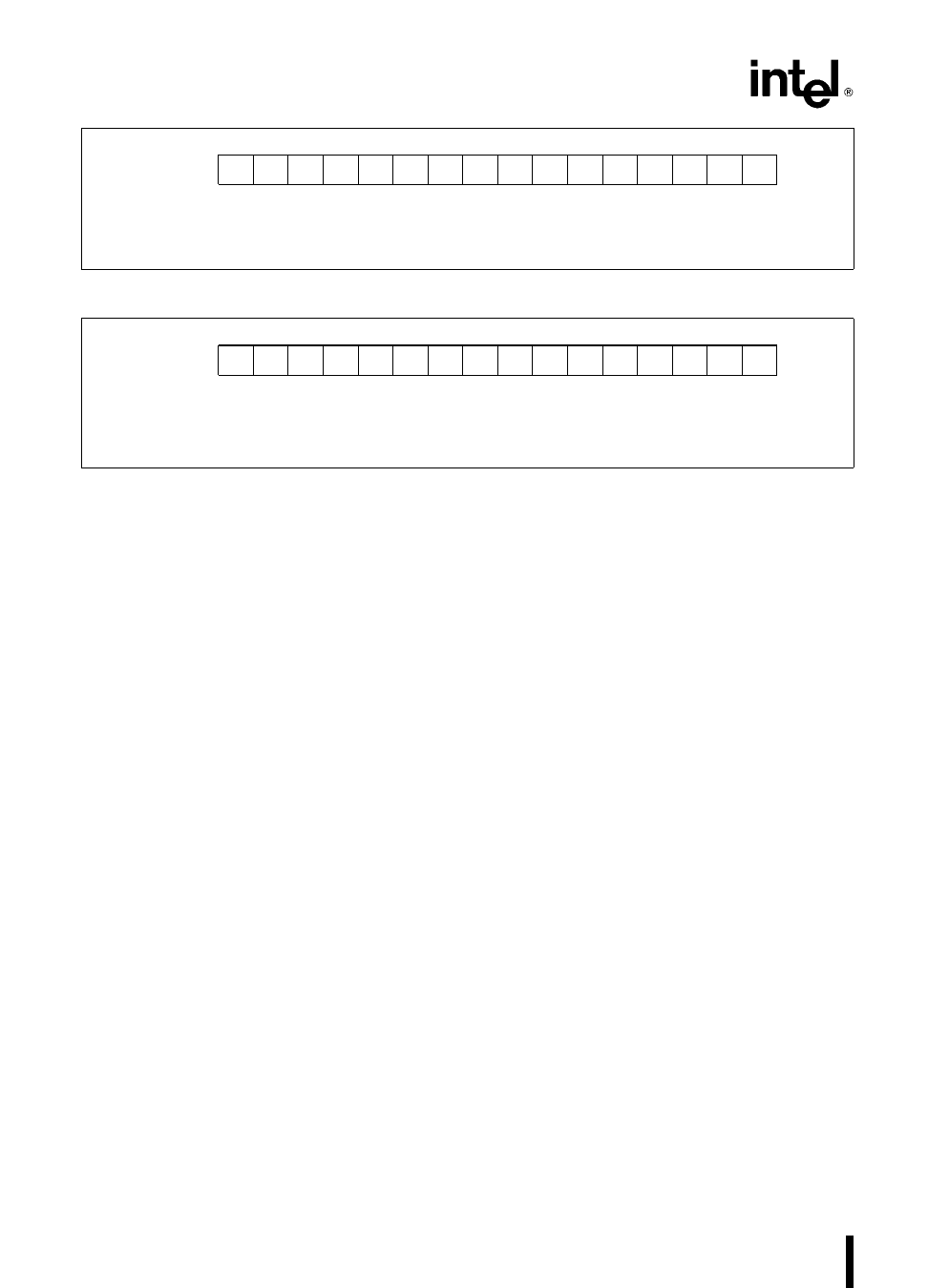
15 14 13 12 11 10 9 8 7 6 5 4 3 2 1 0
CDRAM
0 0 0 0 0 0 0 C8 C7 C6 C5 C4 C3 C2 C1 C0
Offset E2H
Bits 0–8 C0– C8 clock divisor register holds the number of CLKOUT cycles between each refresh
request
Bits 9–15 Reserved read back as 0
Figure 42 Clock Pre-Scaler Register
15 14 13 12 11 10 9 8 7 6 5 4 3 2 1 0
EDRAM
E 0 0 0 0 0 0 T8 T7 T6 T5 T4 T3 T2 T1 T0
Offset E4H
Bits 0–8
Bits 9–14
Bit 15
T0– T8 refresh clock counter outputs Read only
Reserved read back as 0
Enable RCU set to 0 on RESET
Figure 43 Enable RCU Register
Refresh Control Unit Programming and
Operation
After programming the MDRAM and the CDRAM
registers (Figures 40 and 42) the RCU is enabled by
setting the ‘‘E’’ bit in the EDRAM register (Figure
43) The clock counter (T0–T8 of EDRAM) will be
loaded from C0 – C8 of CDRAM during T3 of instruc-
tion cycle that sets the ‘‘E’’ bit The clock counter is
then decremented at each subsequent CLKOUT
frequency is also available at the CLKOUT pin The
PDCON register contains the two-bit fields for se-
lecting the clock division factor and the enable bit
All internal logic including the Refresh Control Unit
and the timers will have their clocks slowed down
by the division factor To maintain a real time count
or a fixed DRAM refresh rate these peripherals must
be re-programmed when entering and leaving the
power-save mode
A refresh is requested when the value of the counter
has reached 1 and the counter is reloaded from
CDRAM In order to avoid missing refresh requests
the value in the CDRAM register should always be at
least 18 (12H) Clearing the ‘‘E’’ bit at anytime will
clear the counter and stop refresh requests but will
not reset the refresh address counter
POWER-SAVE CONTROL
The power-save mode is exited whenever an inter-
rupt is processed by automatically resetting the en-
able bit If the power-save mode is to be re-entered
after serving the interrupt the enable bit will need to
be reset in software before returning from the inter-
rupt routine
The internal clocks of the M80C186 will begin to be
divided during the T3 state of the instruction cycle
that sets the enable bit Clearing the enable bit will
restore full speed in the T3 state of that instruction
Power Save Operation
The M80C186 when in Enhanced Mode can enter
a power saving state by internally dividing the clock-
in frequency by a programmable factor This divided
At no time should the internal clock frequency be
allowed to fall below 0 5 MHz This is the minimum
operational frequency of the M80C186 For exam-
ple an M80C186 running with a 12 MHz crystal
(6 MHz CLOCKOUT) should never have a clock divi-
sor greater than eight
42
Share Link: 