A8438 Ver la hoja de datos (PDF) - Allegro MicroSystems
Número de pieza
componentes Descripción
Fabricante
A8438 Datasheet PDF : 15 Pages
| |||
A8438
Photoflash Capacitor Charger with IGBT Driver
Functional Description
Overview
The A8438 is a photoflash capacitor charger control IC with
adjustable input current limiting. It also integrates an IGBT
driver for strobe operation of the flash tube, dramatically saving
board space in comparison to discrete solutions for strobe flash
operation. The control logic is shown in the functional block
diagram.
The charging operation of the A8438 is started by a low-to-high
signal on the CHARGE pin, provided that VIN is above VUVLO
level. If CHARGE is already high before VIN reaches VUVLO ,
another low-to-high transition on the CHARGE pin is required
to start the charging. When a charging cycle is initiated, the
transformer primary side current, IPrimary, ramps up linearly at a
rate determined by the combined effect of the battery voltage,
VBATT , and the primary side inductance, LPrimary. When IPrimary
reaches the current limit, ISWLIM , set by configuring the ILIM
pin, the internal MOSFET is turned off immediately, allowing the
energy to be pushed into the photoflash capacitor, COUT, from the
secondary winding. The secondary side current drops linearly as
COUT charges.
While the internal MOSFET switch is turned off, the output
voltage, VOUT, is sensed by a resistor string, R1 through R3, con-
nected between the anode of the output diode, D1, and ground.
This resistor string forms a voltage divider that feeds back to the
FB pin. The resistors must be sized to achieve a desired output
voltage level based on a typical value of 1.205 V at the FB pin.
As soon as VOUT reaches the desired value, the charging process
is terminated. The user may toggle the CHARGE pin to refresh
the photoflash capacitor.
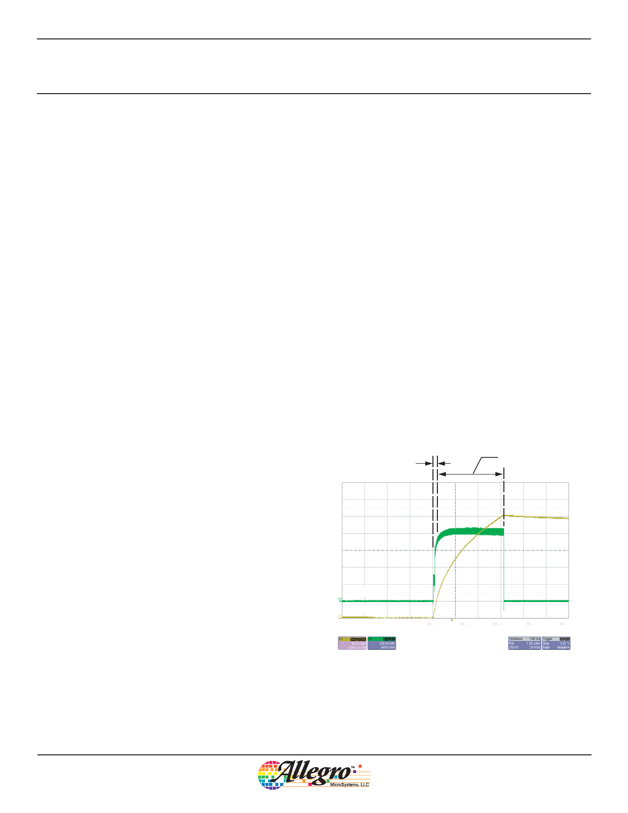
Fast Charging and Timer Modes
The IC operates in the Fast Charging mode when the photoflash
capacitor, COUT, is only partially discharged. In Fast Charging
mode, the converter operates near the discontinuous bound-
ary, and a sensing circuit tracks the fly-back voltage at the SW
node. As soon as this voltage swings below 1.2 V, the internal
MOSFET switch is turned on again, starting the next charging
cycle.
The IC operates in the Timer mode when beginning to charge a
completely discharged photoflash capacitor, usually when the out-
put voltage, VOUT, is less than approximately 10 to 20 V. Timer
mode is a fixed 18 μs off-time control. One advantage of the
A8438 watchdog timer control scheme is that it limits the initial
current surge and thus acts as a “soft-start.” As shown in figure 3,
the timer mode only lasts a small fraction of a second (usually <
100 ms). It can be recognized by its lower initial input charging
current as a result of a lower duty cycle. As output voltage rises to
more than 10 to 20 V, the adaptive Fast Charging mode takes over
the control, raising the average input current level.
Timer
Mode
Fast Charging Mode
Switch On-Time and Off-Time Control
The A8438 implements an adaptive on-time/off-time control. (For
circuit details, please refer to the the Control Logic block in the
simplified Functional Block Diagram on page 2.) On-time dura-
tion, tON , is determined by input voltage, VIN, transformer primary
inductance, LPrimary, and the set current limit, ISWLIM . Off-time
duration, tOFF , depends on the operating conditions during switch
off-time. The A8438 applies its two charging modes, Fast Charg-
ing mode and Timer mode, according to those conditions.
IBATT(Avg)
VOUT
Figure 3. Sequencing of Timer mode and Fast Charging mode (time
axis scale is 1 s per division)
Allegro MicroSystems, LLC
11
115 Northeast Cutoff, Box 15036
Worcester, Massachusetts 01615-0036 (508) 853-5000
www.allegromicro.com
Share Link: 