NCV70522MN(2012) Ver la hoja de datos (PDF) - ON Semiconductor
Número de pieza
componentes Descripción
Fabricante
NCV70522MN Datasheet PDF : 29 Pages
| |||
NCV70522MN
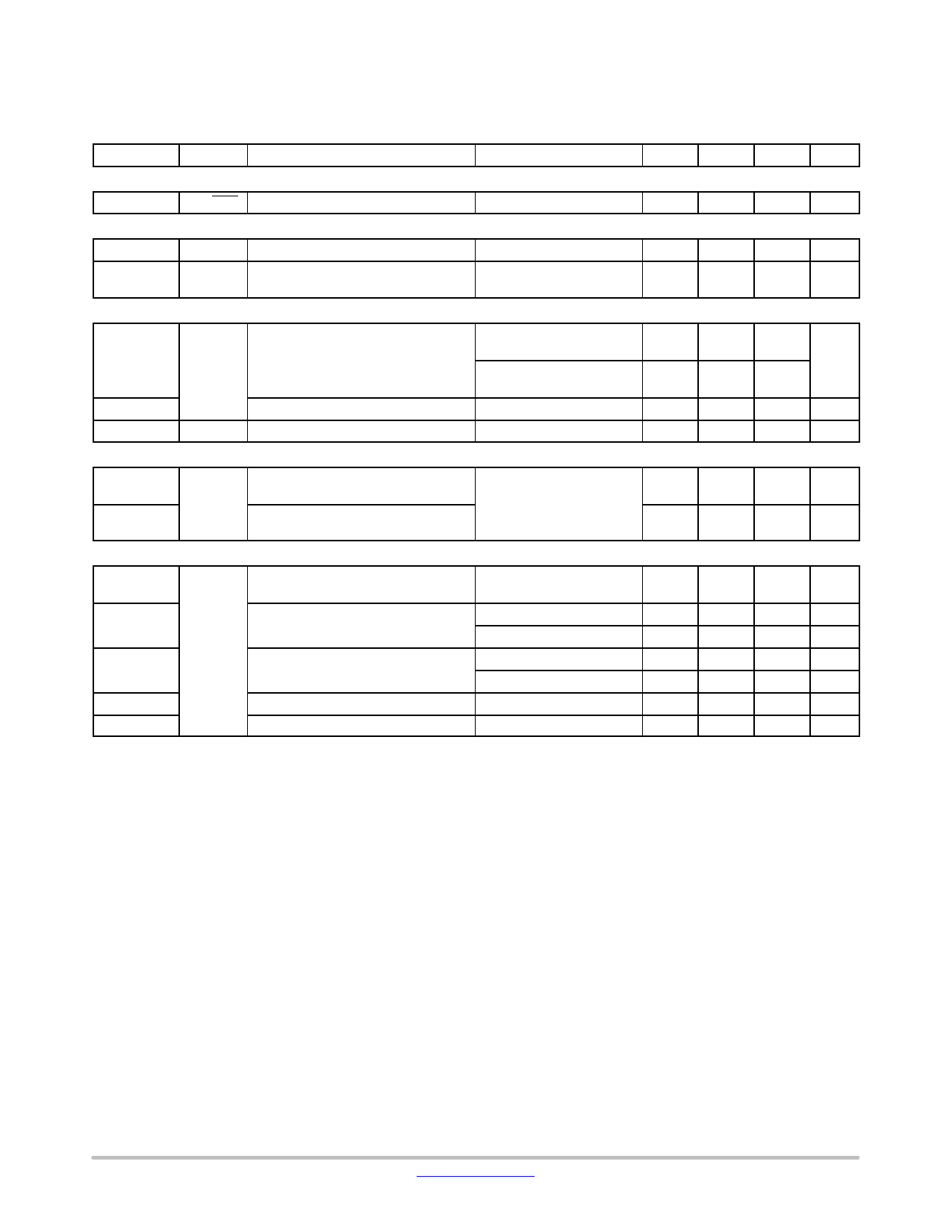
Table 5. DC PARAMETERS
(The DC Parameters are Given for VBB and Temperature in Their Operating Ranges Unless Otherwise Specified)
Convention: Currents Flowing in the Circuit are Defined as Positive.
Symbol
Pin(s)
Parameter
Remark/Test Conditions Min
Typ
Max Unit
DIGITAL OUTPUTS
VOL
DO, ERR Logic Low Level Open Drain
THERMAL WARNING AND SHUTDOWN
Ttw
Ttsd
(Notes 11, 12)
Thermal Warning
Thermal Shutdown
IOL = 5 mA
0.30
V
138
145
152
°C
Ttw + 20
°C
CHARGE PUMP
Vcp
Output Voltage
VCP
6 V ≤ VBB ≤ 14 V
14 V < VBB ≤ 30 V
2 * VBB
− 2.5
V
VBB + 9
VBB +
16
Cbuffer
External Buffer Capacitor
Cpump
CPP CPN External Pump Capacitor
PACKAGE THERMAL RESISTANCE VALUES
180
220
470
nF
180
220
470
nF
Rthja
Rthjp
NQFP
Thermal Resistance
Junction−to−Ambient
Thermal Resistance
Junction−to−Exposed Pad
30
Simulated Conform JEDEC
JESD−51, (2S2P)
0.95
K/W
K/W
SPEED AND LOAD ANGLE OUTPUT
Vout
Output Voltage Range
0.2
VDD −
0.2
V
Voff
Output Offset SLA Pin
SLA
Gsla
Gain of SLA Pin = VBEMF / VCOIL
Rout
Output Resistance SLA Pin
Cload
Load Capacitance SLA Pin
11. No more than 100 cumulative hours in life time above Ttw.
12. Thermal shutdown is derived from Thermal Warning.
SLAG = 0
SLAG = 1
SLAG = 0
SLAG = 1
−50
50
mV
−50
50
mV
0.5
0.25
0.23
1.0
kW
50
pF
http://onsemi.com
7
Share Link: 