MPC9600AE Ver la hoja de datos (PDF) - Integrated Device Technology
Número de pieza
componentes Descripción
Fabricante
MPC9600AE Datasheet PDF : 15 Pages
| |||
MPC9600 Data Sheet
LOW VOLTAGE, 2.5V AND 3.3V LVCMOS PLL CLOCK DRIVER
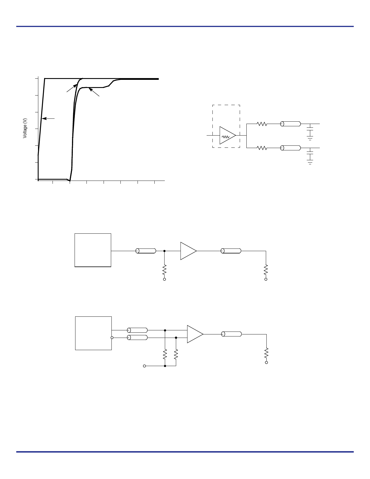
At the load end the voltage will double due to the near unity
reflection coefficient, to 2.6 V. It will then increment towards the
quiescent 3.0 V in steps separated by one round trip delay (in this
case 4.0 ns).
3.0
OutA
2.5
tD = 3.8956
2.0
In
1.5
OutB
tD = 3.9386
1.0
0.5
0
2
4
6
8
10
12
14
Time (ns)
Figure 9. Single versus Dual Waveforms
Since this step is well above the threshold region it will not
cause any false clock triggering, however designers may be
uncomfortable with unwanted reflections on the line. To better
match the impedances when driving multiple lines the situation in
Figure 10 should be used. In this case the series terminating
resistors are reduced such that when the parallel combination is
added to the output buffer impedance the line impedance is
perfectly matched.
MPC9600
Output
Buffer
14
RS = 22 ZO = 50
RS = 22 ZO = 50
14 + 22 || 22 = 50 || 50
25 = 25
Figure 10. Optimized Dual Line Termination
The following figures illustrate the measurement reference for
the MPC9600 clock driver circuit.
Pulse
Generator
Z = 50
ZO = 50
MPC9600 DUT
ZO = 50
RT = 50
RT = 50
VTT
VTT
Figure 11. CCLK MPC9600 AC Test Reference
Differential Pulse
Generator
Z = 50
ZO = 50
MPC9600 DUT
ZO = 50
RT = 50
RT = 50
VTT
VTT
Figure 12. PCLK MPC9600 AC Test Reference
MPC9600 REVISION 6 JANUARY 7, 2013
11
©2013 Integrated Device Technology, Inc.
Share Link: 