MC33264D-4.75 Ver la hoja de datos (PDF) - ON Semiconductor
Número de pieza
componentes Descripción
Fabricante
MC33264D-4.75 Datasheet PDF : 10 Pages
| |||
MC33264
ELECTRICAL CHARACTERISTICS (continued) (Vin = 6.0 V, IO = 10 mA, CO = 1.0 μF, TJ = 25°C (Note 1), unless otherwise noted.)
Characteristic
Symbol
Min
Typ
Max
Unit
ON/OFF INPUTS
ÁÁÁÁÁÁÁÁÁÁÁÁÁÁÁÁÁÁÁÁÁÁÁÁÁÁÁÁÁÁÁÁÁ On/Off Input (Pin 3 Tied to Ground)
ÁÁÁÁÁÁÁÁÁÁÁÁÁÁÁÁÁÁÁÁÁÁÁÁÁÁÁÁÁÁÁÁÁ Logic “1” (Regulator ON)
VOn/Off
V
2.4
−
Vin
Logic “0” (Regulator OFF)
0
−
0.5
On/Off Input (Pin 2 Tied to Vin)
Logic “0” (Regulator ON)
Logic “1” (Regulator OFF)
ÁÁÁÁÁÁÁÁÁÁÁÁÁÁÁÁÁÁÁÁÁÁÁÁÁÁÁÁÁÁÁÁÁ On/Off Pin Input Current (Pin 3 Tied to Ground)
ÁÁÁÁÁÁÁÁÁÁÁÁÁÁÁÁÁÁÁÁÁÁÁÁÁÁÁÁÁÁÁÁÁ VOn/Off= 2.4 V
IOn/Off
0
Vin − 0.2
−
−
Vin − 2.4
−
Vin
μA
1.9
−
On/Off Pin Input Current (Pin 2 Tied to Vin)
VOn/Off = Vin − 2.4 V
−
12
−
NOTES: 1. Low duty pulse techniques are used during test to maintain junction temperature as close to ambient as possible.
2. Quiescent current is measured where the PNP pass transistor is in saturation. VCE = −0.5 V guarantees this condition.
3. Noise tests on the MC33264 are made with a 0.01 μF capacitor connected across Pins 8 and 5.
DEFINITIONS
Dropout Voltage − The input/output voltage differential
at which the regulator output no longer maintains regulation
against further reductions in input voltage. Measured when
the output drops 100 mV below its nominal value (which is
measured at 1.0 V differential), dropout voltage is affected
by junction temperature, load current and minimum input
supply requirements.
Line Regulation − The change in output voltage for a
change in input voltage. The measurement is made under
conditions of low dissipation or by using pulse techniques such
that average chip temperature is not significantly affected.
Load Regulation − The change in output voltage for a
change in load current at constant chip temperature.
Maximum Power Dissipation − The maximum total
device dissipation for which the regulator will operate
within specifications.
Quiescent Current − Current which is used to operate the
regulator chip and is not delivered to the load.
Output Noise Voltage − The rms ac voltage at the output,
with constant load and no input ripple, measured over a
specified frequency range.
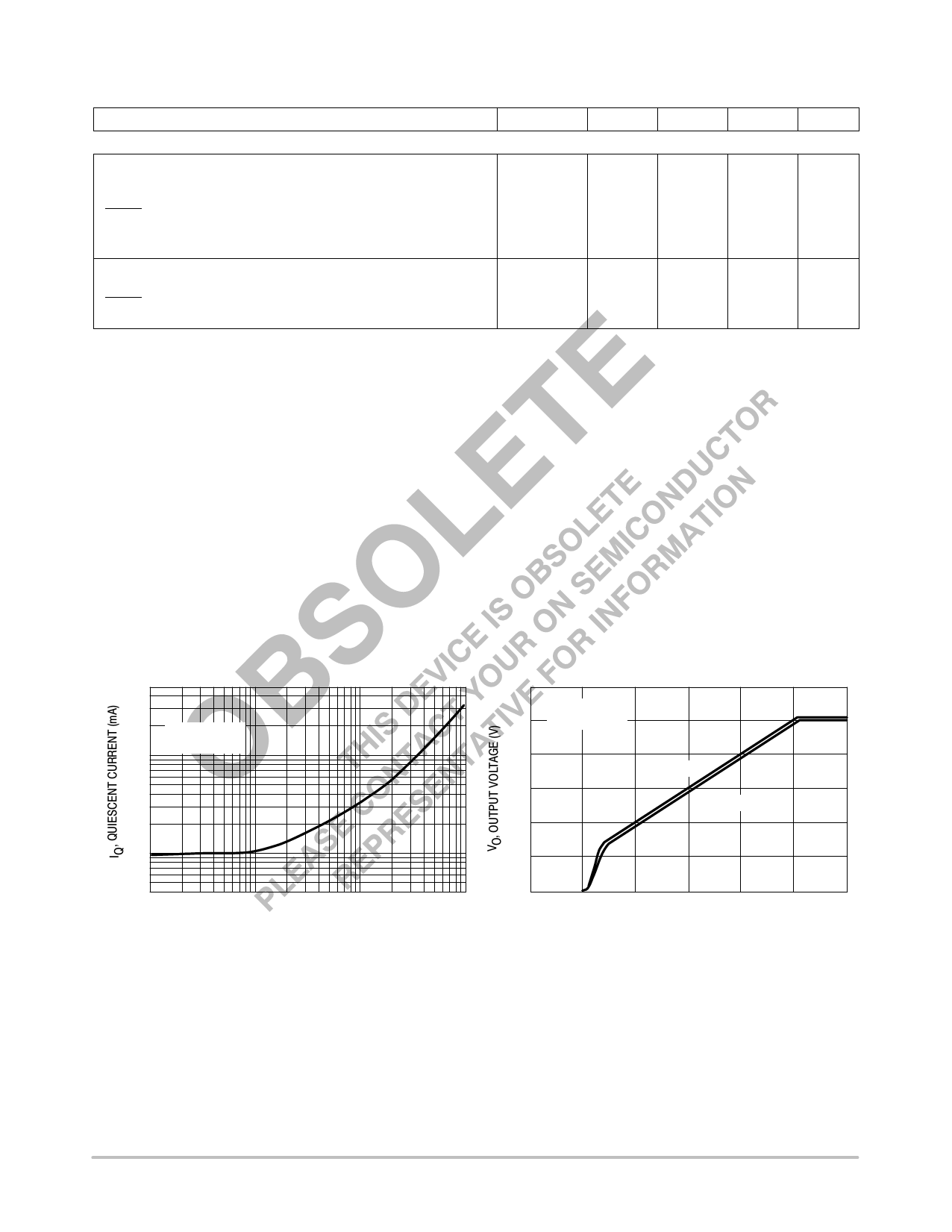
5.0
TA = 25°C
MC33264D−5.0
1.0
0.10
0.03
0.1
1.0
10
Iload, LOAD CURRENT (mA)
Figure 1. Quiescent Current
versus Load Current
6.0
TA = 25°C
5.0 MC33264D−5.0
4.0
RL = 5.0 k
3.0
RL = 100 Ω
2.0
1.0
0
100
0
1.0
2.0
3.0
4.0
5.0
6.0
Vin, INPUT VOLTAGE (V)
Figure 2. Output Voltage versus Input Voltage
http://onsemi.com
4
Share Link: 