APA3160A Ver la hoja de datos (PDF) - Anpec Electronics
Número de pieza
componentes Descripción
Fabricante
APA3160A Datasheet PDF : 38 Pages
| |||
APA3160A
Function Description (Cont.)
Power-down Sequence
Use the following sequence to power-down the device and its supplies:
1. If time permits, enter shutdown (sequence defined above); else, in case of sudden power loss, assert SD=0 and
wait at least 2ms.
2. Assert RST=0.
3. Drive digital inputs low and ramp down PVDD supply as follows:
• Drive all digital inputs low after RST has been low for at least 2µs.
• Ramp down PVDD while ensuring that it remains above 8V until RST has been low for at least 2µs.
4. Ramp down AVDD/DVDD while ensuring that it remains above 3V until PVDD is below 6V and that it is never more
than 2.5V below the digital inputs.
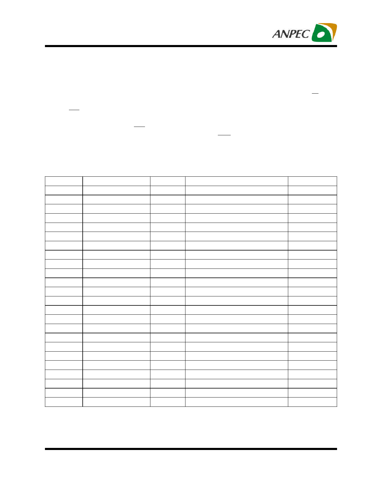
Table 1. Serial Control Interface Register Summary
Sub Address
Register Name
No. of Bytes
Contents
A u indicates unused bits.
0x00
Clock control register
1
Description shown in subsequent section
0x02
Error status register
1
Description shown in subsequent section
0x03
System control register 1
1
Description shown in subsequent section
0x04
Serial data interface
1
Description shown in subsequent section
0x05
1
Description shown in subsequent section
0x06
Soft mute register
1
Description shown in subsequent section
0x07
Master volume
1
Description shown in subsequent section
0x08
Channel 1 vol
1
Description shown in subsequent section
0x09
Channel 2 vol
1
Description shown in subsequent section
0x0A
0x0B - 0X0D
Fine master volume
1
Description shown in subsequent section
Reserved (Note 4)
0x0E
Volume configuration register
1
Description shown in subsequent section
0x0F
1
Reserved (Note 4)
0x10
0x15-0x19
Modulation limit register
1
Description shown in subsequent section
1
Reserved (Note 4)
0x1A
0x1B
0x1C
0x1D–0x1F
Start/stop period register
1
Description shown in subsequent section
1
Reserved (Note 4)
1
Reserved (Note 4)
1
Reserved (Note 4)
0x20
0x21-0x24
Input MUX register
1
Description shown in subsequent section
1
Reserved (Note 4)
0x25
0x26-0xFF
PWM MUX register
1
Description shown in subsequent section
1
Reserved (Note 4)
Note 4: Reserved register should not be accessed.
Initialization Values
0x6C
0x00
0x80
0x05
0x40
0x00
0xFF (mute)
0x30 (0dB)
0x30 (0dB)
0x00 (0dB)
0x91
0x02
0x0F
0x 89
0x27
Copyright © ANPEC Electronics Corp.
21
Rev. A.6 - Jan., 2013
www.anpec.com.tw
Share Link: 