HI-5700/883 Ver la hoja de datos (PDF) - Intersil
Número de pieza
componentes Descripción
Fabricante
HI-5700/883 Datasheet PDF : 8 Pages
| |||
Specifications HI-5700/883
Absolute Maximum Ratings
Thermal Information
Supply Voltage, VDD to GND . . . . . . . . . (GND - 0.5) < VDD < +7.0V
Analog and Reference Input Pins. .(VSS - 0.5) < VINA < (VDD +0.5V)
Digital I/O Pins . . . . . . . . . . . . . . . (GND - 0.5) < VI/O < (VDD +0.5V)
Operating Temperature Range
HI1-5700S/883 . . . . . . . . . . . . . . . . . . . . . . . . . . -55oC to +125oC
Junction Temperature. . . . . . . . . . . . . . . . . . . . . . . . . . . . . . +175oC
Storage Temperature Range . . . . . . . . . . . . . . . -65oC to +150oC
Lead Temperature (Soldering, 10s) . . . . . . . . . . . . . . . . . . . . 300oC
ESD Clasification . . . . . . . . . . . . . . . . . . . . . . . . . . . . . . . . . Class 1
Thermal Resistance
HI1-5700S/883 . . . . . . . . . . . . . . . . . . . .
Power Dissipation at +75oC (Note 1)
θJA
470C/W
θJC
28oC/W
HI1-5700S/883 . . . . . . . . . . . . . . . . . . . . . . . . . . . . . . . . 2100mW
Power Dissipation Derating Factor Above +75oC
HI1-5700S/883 . . . . . . . . . . . . . . . . . . . . . . . . . . . . . . . 21mW/oC
Reliabiliy Information
Transistor Count . . . . . . . . . . . . . . . . . . . . . . . . . . . . . . . . . . . 14677
Worst Case Density . . . . . . . . . . . . . . . . . . . . . . . . 3.05 x 10⁴A/cm2
CAUTION: Stresses above those listed in “Absolute Maximum Ratings” may cause permanent damage to the device. This is a stress only rating and operation
of the device at these or any other conditions above those indicated in the operational sections of this specification is not implied.
Device Tested at:
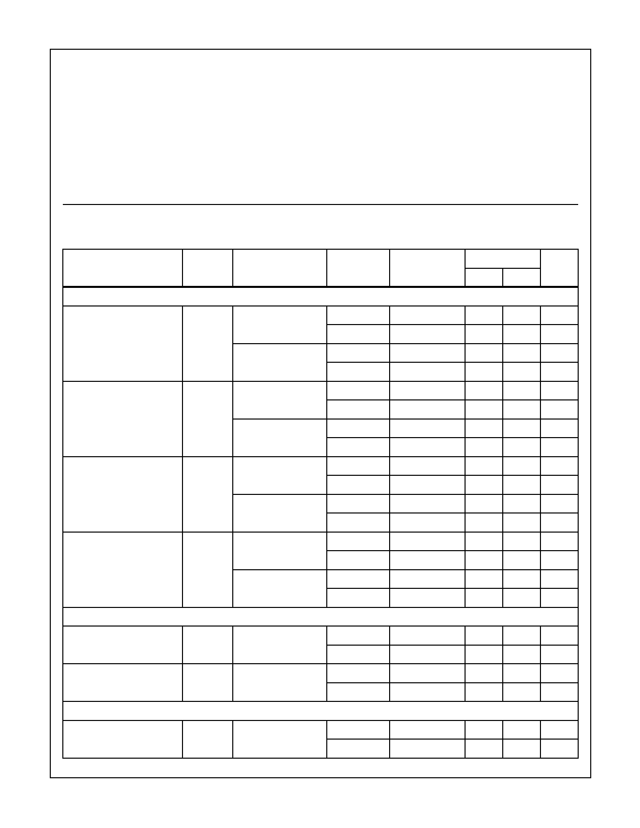
TABLE 1. DC ELECTRICAL PERFORMANCE CHARACTERISTICS
AVDD = VDD = +5.0V; VREF+ = +4.0V; VREF- = GND = AGND = 0V; FS = Specified Clock Frequency at 50% Duty Cycle;
CL = 30pF; Unless Otherwise Specified.
PARAMETERS
SYMBOL
CONDITIONS
GROUP A
SUBGROUP TEMPERATURE
LIMITS
MIN MAX
UNIT
ACCURACY
Integral Linearity Error
(Best Fit Method)
Differential Linearity Error
(Guaranteed No Missing
Codes)
Offset Error
(Adjustable to Zero)
Full Scale Error
(Adjustable to Zero)
INL
FS = 15MHz, fIN = DC
1
2, 3
FS = 20MHz, fIN = DC
1
2, 3
DNL
FS = 15MHz, fIN = DC
1
2, 3
FS = 20MHz, fIN = DC
1
2, 3
VOS
FS = 15MHz, fIN = DC
1
2, 3
FS = 20MHz, fIN = DC
1
2, 3
FSE
FS = 15MHz, fIN = DC
1
2, 3
FS = 20MHz, fIN = DC
1
2, 3
+25oC
-
±2.0
LSB
+125oC, -55oC
-
±2.65 LSB
+25oC
-
±2.25 LSB
+125oC, -55oC
-
±4.1
LSB
+25oC
-
±0.9
LSB
+125oC, -55oC
-
±1.0
LSB
+25oC
-
±0.9
LSB
+125oC, -55oC
-
±1.0
LSB
+25oC
-
±8.0
LSB
+125oC, -55oC
-
±9.5
LSB
+25oC
-
±8.0
LSB
+125oC, -55oC
-
±9.5
LSB
+25oC
-
±4.5
LSB
+125oC, -55oC
-
±8.0
LSB
+25oC
-
±4.5
LSB
+125oC, -55oC
-
±8.0
LSB
ANALOG INPUT
Analog Input Resistance
Analog Input Bias Current
RIN
VIN = 4V
IB
VIN = 0V, 4V
1
+25oC
4
-
MΩ
2, 3
+125oC, -55oC
4
-
MΩ
1
+25oC
±1.0
µA
2, 3
+125oC, -55oC
±1.0
µA
REFERENCE INPUT
Total Reference Resistance
RL
1
+25oC
250
-
Ω
2, 3
+125oC, -55oC
235
-
Ω
Spec Number 512023
6-10
Share Link: 