MC100LVEL31(2016) Ver la hoja de datos (PDF) - ON Semiconductor
Número de pieza
componentes Descripción
Fabricante
MC100LVEL31 Datasheet PDF : 6 Pages
| |||
MC100LVEL31
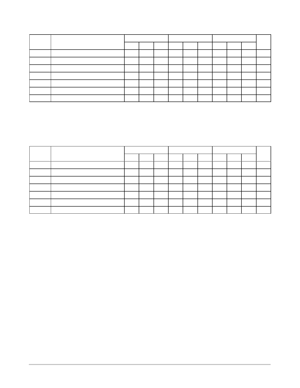
Table 4. LVPECL DC CHARACTERISTICS (VCC = 3.3 V; VEE = 0.0 V (Note 1))
−40°C
25°C
85°C
Symbol
Characteristic
Min Typ Max Min Typ Max Min Typ Max Unit
IEE
Power Supply Current
VOH
Output HIGH Voltage (Note 2)
VOL
Output LOW Voltage (Note 2)
VIH
Input HIGH Voltage
VIL
Input LOW Voltage
IIH
Input HIGH Current
IIL
Input LOW Current
30
35
30
35
32
38
mA
2215 2295 2420 2275 2345 2420 2275 2345 2420 mV
1470 1605 1745 1490 1595 1680 1490 1595 1680 mV
2135
2420 2135
2420 2135
2420 mV
1490
1825 1490
1825 1490
1825 mV
150
150
150 mA
0.5
0.5
0.5
mA
NOTE: Device will meet the specifications after thermal equilibrium has been established when mounted in a test socket or printed circuit
board with maintained transverse airflow greater than 500 lfpm. Electrical parameters are guaranteed only over the declared
operating temperature range. Functional operation of the device exceeding these conditions is not implied. Device specification limit
values are applied individually under normal operating conditions and not valid simultaneously.
1. Input and output parameters vary 1:1 with VCC. VEE can vary ±0.3 V.
2. Outputs are terminated through a 50 W resistor to VCC − 2.0 V.
Table 5. LVNECL DC CHARACTERISTICS (VCC = 0.0 V; VEE = −3.3 V (Note 1))
−40°C
25°C
85°C
Symbol
Characteristic
Min Typ Max Min Typ Max Min Typ Max Unit
IEE
Power Supply Current
VOH
Output HIGH Voltage (Note 2)
VOL
Output LOW Voltage (Note 2)
VIH
Input HIGH Voltage
VIL
Input LOW Voltage
IIH
Input HIGH Current
IIL
Input LOW Current
30
35
30
35
32
38
mA
−1085 −1005 −880 −1025 −955 −880 −1025 −955 −880 mV
−1830 −1695 −1555 −1810 −1705 −1620 −1810 −1705 −1620 mV
−1165
−880 −1165
−880 −1165
−880 mV
−1810
−1475 −1810
−1475 −1810
−1475 mV
150
150
150 mA
0.5
0.5
0.5
mA
NOTE: Device will meet the specifications after thermal equilibrium has been established when mounted in a test socket or printed circuit
board with maintained transverse airflow greater than 500 lfpm. Electrical parameters are guaranteed only over the declared
operating temperature range. Functional operation of the device exceeding these conditions is not implied. Device specification limit
values are applied individually under normal operating conditions and not valid simultaneously.
1. Input and output parameters vary 1:1 with VCC. VEE can vary ±0.3 V.
2. Outputs are terminated through a 50 W resistor to VCC − 2.0 V.
www.onsemi.com
3
Share Link: 