NX25P10 Ver la hoja de datos (PDF) - NexFlash -> Winbond Electronics
Número de pieza
componentes Descripción
Fabricante
NX25P10 Datasheet PDF : 28 Pages
| |||
1M / 2M / 4M-BIT SERIAL FLASH MEMORY with 40MHz SPI
NX25P10, NX25P20 AND NX25P40
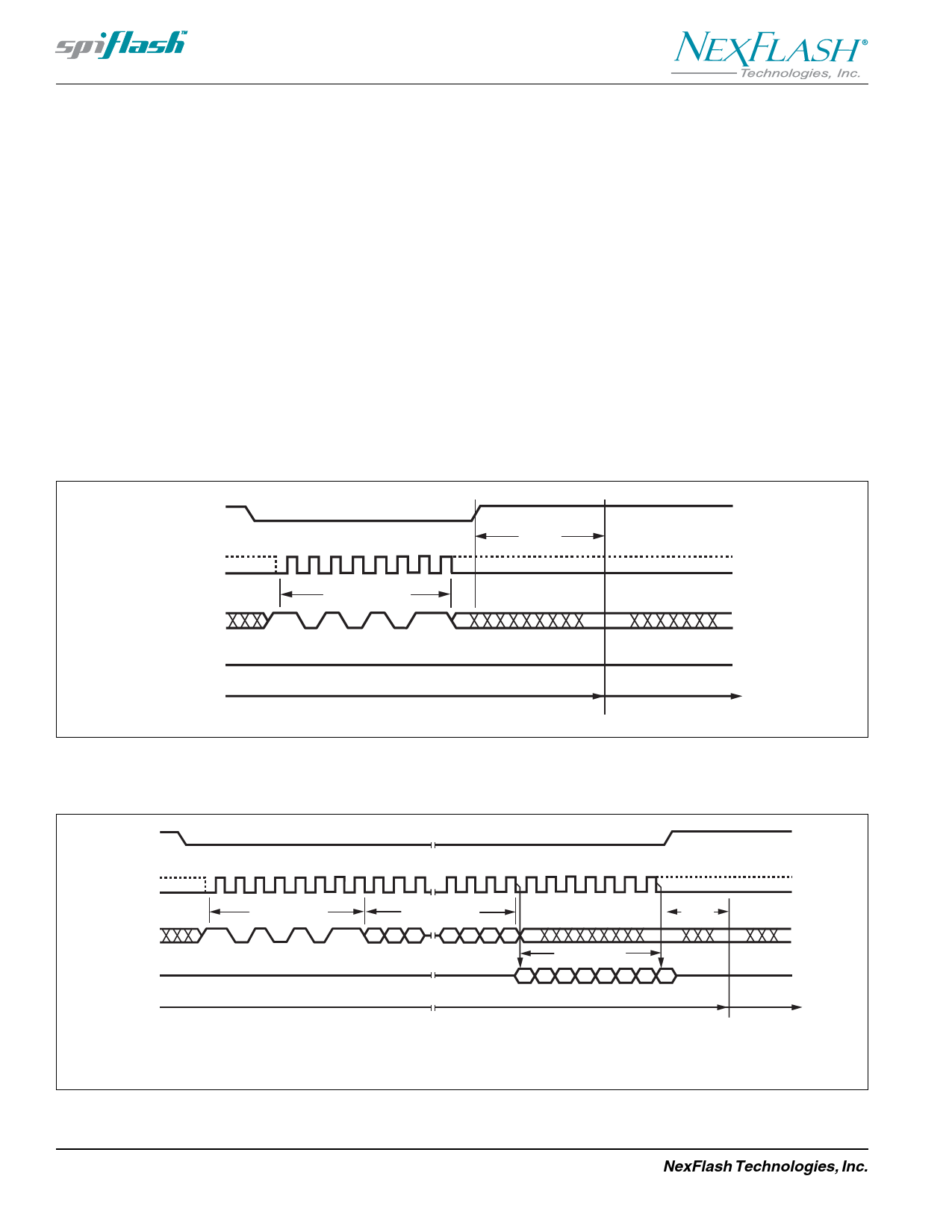
Release Power-down / Device ID (ABh)
The Release from Power-down / Device ID instruction is a
multi-purpose instruction. It can be used to release the
device from the power-down state, obtain the devices
electronic identification (ID) number or do both.
first as shown in figure 15. The Device ID values for the
NX25P10, NX25P20, and NX25P40 are listed in Table 4.
The Device ID can be read continuously. The instruction is
completed by driving CS high.
When used only to release the device from the power-down
state, the instruction is issued by driving the CS pin low,
shifting the instruction code “ABh” and driving CS high as
shown in figure 14. After the time duration of tRES1 (See AC
Characteristics) the device will resume normal operation
and other instructions will be accepted. The CS pin must
remain high during the tRES1 time duration.
When used to release the device from the power-down state
and obtain the Device ID, the instruction is the same as
previously described, and shown in figure 13, except that
after CS is driven high it must remain high for a time duration
of tRES2 (See AC Characteristics). After this time duration
the device will resume normal operation and other instruc-
tions will be accepted.
When used only to obtain the Device ID while not in the
power-down state, the instruction is initiated by driving the
CS pin low and shifting the instruction code “ABh” followed
by 3-dummy bytes. The Device ID bits are then shifted out
on the falling edge of CLK with most significant bit (MSB)
If the Release from Power-down / Device ID instruction is
issued while an Erase, Program or Write cycle is in process
(when BUSY equals 1) the instruction is ignored and will not
have any effects on the current cycle.
CS
Mode 3
CLK Mode 0
DI
DO
01 2 3 456 7
Instruction (ABh)
High Impedance
tRES1
Power-down Current
Stand-by Current
Figure 14. Release Power-down Instruction Sequence
CS
Mode 3
CLK Mode 0
0 1 2 3 4 5 6 7 8 9 10 28 29 30 31 32 33 34 35 36 37 38
Instruction (ABh)
3 Dummy Bytes
tRES2
DI
23 22 21
32 1 0
*
** Device ID
High Impedance
DO
7 654 321 0
*
Power-down Current
* = MSB
** = See Table 4
Stand-by Current
Figure 15. Release Power-down / Device ID Instruction Sequence Diagram
20
NexFlash Technologies, Inc.
PRELIMINARY MKP-0009 Rev 6 NXSF040I-0405
04/04/05 ©
Share Link: 