NX25P10 Ver la hoja de datos (PDF) - NexFlash -> Winbond Electronics
Número de pieza
componentes Descripción
Fabricante
NX25P10 Datasheet PDF : 28 Pages
| |||
1M / 2M / 4M-BIT SERIAL FLASH MEMORY with 40MHz SPI
NX25P10, NX25P20 AND NX25P40
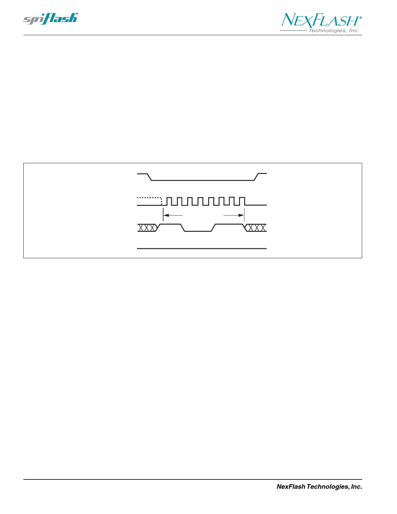
Bulk Erase (C7h)
The Bulk Erase instruction sets all memory within the
device to the erased state of all 1s (FFh). A Write Enable
instruction must be executed before the device will accept
the Bulk Erase Instruction (Status Register bit WEL must
equal 1). The instruction is initiated by driving the CS pin low
and shifting the instruction code “C7h”. The Bulk Erase
instruction sequence is shown in figure 12.
The CS pin must be driven high after the eighth bit has been
latched. If this is not done the Bulk Erase instruction will not
be executed. After CS is driven high, the self-timed Bulk
Erase instruction will commence for a time duration of tBE
(See AC Characteristics). While the Bulk Erase cycle is in
progress, the Read Status Register instruction may still be
accessed to check the status of the BUSY bit. The BUSY
bit is a 1 during the Bulk Erase cycle and becomes a 0 when
finished and the device is ready to accept other instructions
again. After the Bulk Erase cycle has started the Write
Enable Latch (WEL) bit in the Status Register is cleared to
0. The Bulk Erase instruction will not be executed if any
page is protected by the Block Protect (BP2, BP1, BP0) bits
(see Table 2).
CS
Mode 3
CLK Mode 0
DI
01 2 3 4 56 7
Instruction (C7h)
High Impedance
DO
Figure 12. Bulk Erase Instruction Sequence Diagram
18
NexFlash Technologies, Inc.
PRELIMINARY MKP-0009 Rev 6 NXSF040I-0405
04/04/05 ©
Share Link: 