NX25P40-VNI Ver la hoja de datos (PDF) - NexFlash -> Winbond Electronics
Número de pieza
componentes Descripción
Fabricante
NX25P40-VNI
NexFlash -> Winbond Electronics

NX25P40-VNI Datasheet PDF : 28 Pages
| |||
1M / 2M / 4M-BIT SERIAL FLASH MEMORY with 40MHz SPI
NX25P10, NX25P20 AND NX25P40
Write Enable (06h)
The Write Enable instruction (Figure 4) sets the Write
Enable Latch (WEL) bit in the Status Register to a 1. The
WEL bit must be set prior to every Page Program, Sector
Erase, Bulk Erase and Write Status Register instruction.
The Write Enable instruction is entered by driving CS low,
1 shifting the instruction code “06h” into the Data Input (DI) pin
on the rising edge of CLK, and then driving CS high.
2
CS
Mode 3
01 2 3 456 7
3
CLK Mode 0
Instruction (06h)
DI
4
High Impedance
DO
5
Figure 4. Write Enable Instruction Sequence Diagram
6
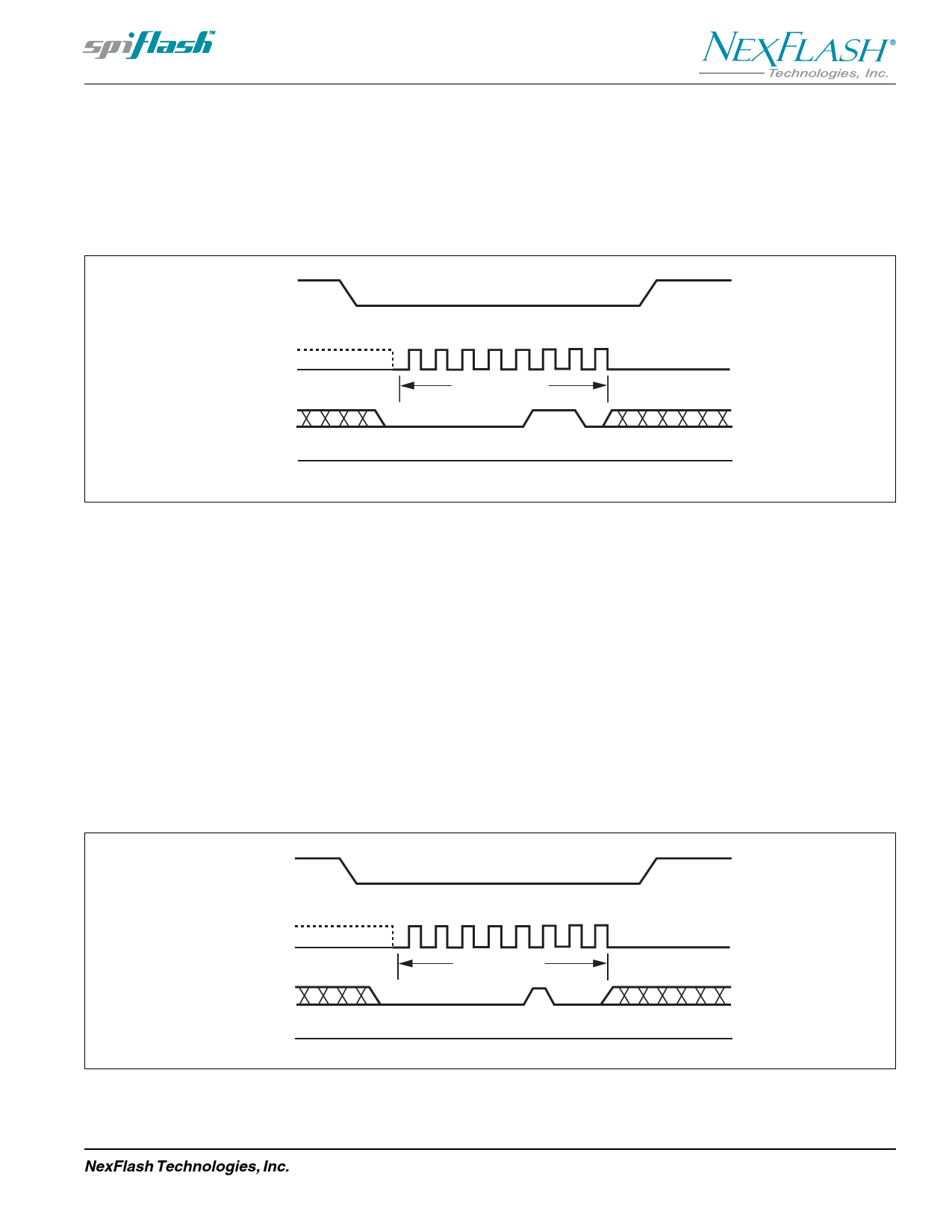
Write Disable (04h)
The Write Disable instruction (Figure 5) resets the Write
Enable Latch (WEL) bit in the Status Register to a 0. The
Write Disable instruction is entered by driving CS low,
shifting the instruction code “04h” into the DI pin and then
7
8 driving CS high. Note that the WEL bit is automatically reset
after Power-up and upon completion of the Write Status
Register, Page Program, Sector Erase, and Bulk Erase
instructions.
9
CS
Mode 3
CLK Mode 0
DI
DO
01 2 3 456 7
Instruction (04h)
High Impedance
Figure 5. Write Disable Instruction Sequence Diagram
10
11
12
NexFlash Technologies, Inc.
11
PRELIMINARY MKP-0009 Rev 6 NXSF040I-0405
04/04/05 ©
Share Link: