LT1168C Ver la hoja de datos (PDF) - Linear Technology
Número de pieza
componentes Descripción
Fabricante
LT1168C
Linear Technology

LT1168C Datasheet PDF : 20 Pages
| |||
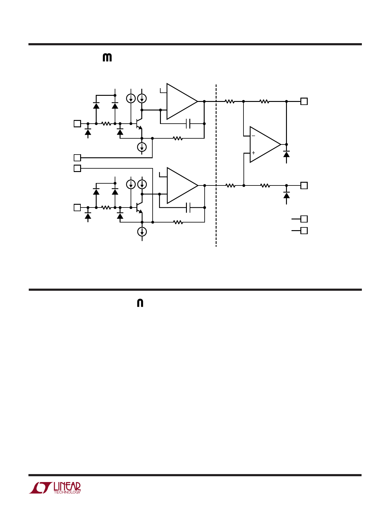
BLOCK DIAGRA
LT1168
+VS
–IN 2
R3
400Ω
–VS
RG 1
RG 8
+VS
+IN 3
R4
400Ω
–VS
VB
+
A1
–
C1
Q1
R1
24.7k
VB
+
A2
–
C2
Q2
R2
24.7k
PREAMP STAGE
R5
R6
30k
30k
6 OUTPUT
–
A3
+
–VS
R7
R8
30k
30k
5 REF
–VS
DIFFERENCE AMPLIFIER STAGE
7 +VS
4 –VS
1168 F01
Figure 1. Block Diagram
U
THEORY OF OPERATIO
The LT1168 is a modified version of the three op amp
instrumentation amplifier. Laser trimming and monolithic
construction allow tight matching and tracking of circuit
parameters over the specified temperature range. Refer to
the block diagram (Figure 1) to understand the following
circuit description. The collector currents in Q1 and Q2 are
trimmed to minimize offset voltage drift, thus assuring a
high level of performance. R1 and R2 are trimmed to an
absolute value of 24.7k to assure that the gain can be set
accurately (0.6% at G = 100) with only one external
resistor RG. The value of RG in parallel with R1 (R2)
determines the transconductance of the preamp stage. As
RG is reduced for larger programmed gains, the transcon-
ductance of the input preamp stage increases to that of the
input transistors Q1 and Q2. This increases the open-loop
gain when the programmed gain is increased, reducing
the input referred gain related errors and noise. The input
voltage noise at gains greater than 50 is determined only
by Q1 and Q2. At lower gains the noise of the difference
amplifier and preamp gain setting resistors increase the
noise. The gain bandwidth product is determined by C1,
C2 and the preamp transconductance which increases
with programmed gain. Therefore, the bandwidth does not
drop proportionally with gain.
The input transistors Q1 and Q2 offer excellent matching,
which is inherent in NPN bipolar transistors, as well as
picoampere input bias current due to superbeta process-
ing. The collector currents in Q1 and Q2 are held constant
due to the feedback through the Q1-A1-R1 loop and
Q2-A2-R2 loop which in turn impresses the differential
input voltage across the external gain set resistor RG.
Since the current that flows through RG also flows through
R1 and R2, the ratios provide a gained-up differential
11
Share Link: