LT1168C Ver la hoja de datos (PDF) - Linear Technology
Número de pieza
componentes Descripción
Fabricante
LT1168C
Linear Technology

LT1168C Datasheet PDF : 20 Pages
| |||
U
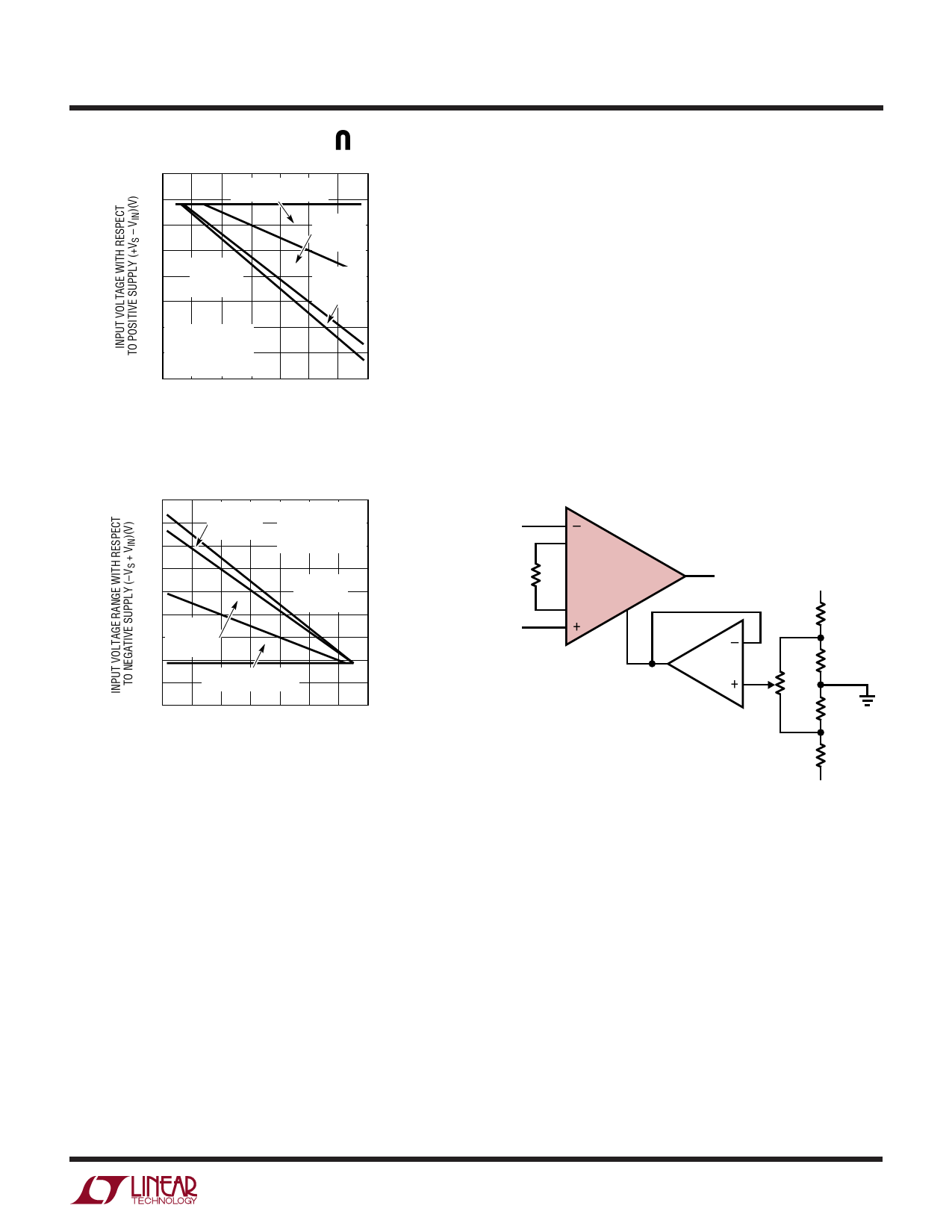
THEORY OF OPERATIO
+VS
G=1
–1
AREA OF OPERATION
–2
–3
G = 100
–4
AREA OF
OPERATION
–5
G=2
AREA OF
OPERATION
G = 10
AREA OF
OPERATION
–6 TA = 25°C
INPUT COMMON
–7 MODE RANGE IS
BELOW THE CURVE
–8
02 4 6
8 10 12 14
VOUT (V)
1168 F02
Figure 2. Positive Input Range vs
Output Voltage for Different Gains
9
G = 10
TA = 25°C
8
AREA OF
INPUT COMMON
OPERATION MODE RANGE IS
7
ABOVE THE CURVE
6
5
4
G=2
3 AREA OF
OPERATION
2
G = 100
AREA OF
OPERATION
G=1
1
AREA OF OPERATION
–VS
–14 –12 –10 –8 – 6 –4 –2 0
VOUT (V)
1168 F03
Figure 3. Negative Input Voltage Range
vs Output Voltage for Various Gains
Single Supply Operation
For best results under single supply operation, the REF pin
should be raised above the negative supply (Pin 4) and one
of the inputs should be at least 2.5V above ground. The
barometer application later in this data sheet is an example
that satisfies these conditions. The resistance RSET from
the bridge transducer to ground sets the operating current
for the bridge, and with R6, also has the effect of raising the
input common mode voltage. The output of the LT1168 is
always inside the specified range since the barometric
pressure rarely goes low enough to cause the output to clip
(30.00 inches of Hg corresponds to 3.000V). For applica-
tions that require the output to swing at or below the REF
LT1168
potential, the voltage on the REF pin can be further level
shifted. The application in the front of this data sheet,
Single Supply Pressure Monitor, is an example. An op amp
is used to buffer the voltage on the REF pin since a parasitic
series resistance will degrade the CMRR.
Output Offset Trimming
The LT1168 is laser trimmed for low offset voltage so that
no external offset trimming is required for most applica-
tions. In the event that the offset needs to be adjusted, the
circuit in Figure 4 is an example of an optional offset adjust
circuit. The op amp buffer provides a low impedance to the
REF pin where resistance must be kept to minimum for
best CMRR and lowest gain error.
–IN
2–
1
RG
LT1168
8
REF
+IN
3+
5
6
OUTPUT
1/2 LT1112
±10mV
ADJUSTMENT RANGE
+VS
10mV
100Ω
10k
100Ω
–10mV
–VS
1168 F04
Figure 4. Optional Trimming of Output Offset Voltage
Input Bias Current Return Path
The low input bias current of the LT1168 (250pA) and the
high input impedance (200GΩ) allow the use of high
impedance sources without introducing additional offset
voltage errors, even when the full common mode range is
required. However, a path must be provided for the input
bias currents of both inputs when a purely differential
signal is being amplified. Without this path the inputs will
float to either rail and exceed the input common mode
range of the LT1168, resulting in a saturated input stage.
Figure 5 shows three examples of an input bias current
13
Share Link: