87C196LA Ver la hoja de datos (PDF) - Intel
Número de pieza
componentes Descripción
Fabricante
87C196LA Datasheet PDF : 21 Pages
| |||
AUTOMOTIVE — 87C196LA
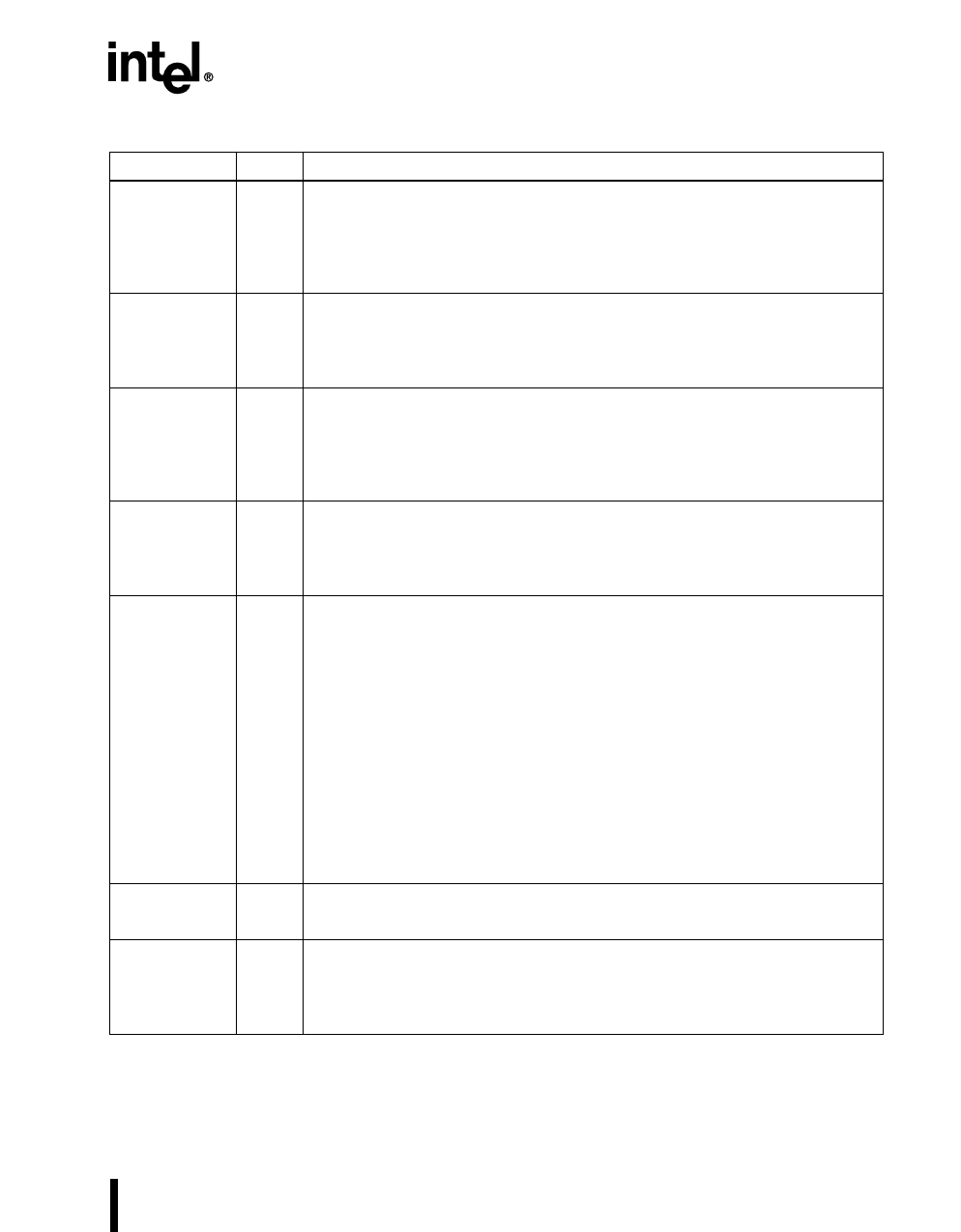
Name
P5.3:2
P5.0
P6.7:4
P6.1:0
PACT#
PALE#
PBUS.15:0
PLLEN
PMODE.3:0
Type
I/O
O
O
I
I/O
I
I
Table 4. Signal Descriptions (Continued)
Description
Port 5
This is a memory-mapped, bidirectional port.
Port 5 shares package pins with the following signals: P5.0/ADV#/ALE,
P5.2/WR#/WRL#/PLLEN, and P5.3/RD#. P5.1 and P5.7:4 are not
implemented.
Port 6
This is a standardbidirectional port.
Port 6 shares package pins with the following signals: P6.0/EPA8/COMP0,
P6.1/EPA9/COMP1, P6.4/SC0, P6.5/SD0, P6.6/SC1, and P6.7/SD1.
Programming Active
During auto programming or slave dump, a low signal indicates that
programming or dumping is in progress, while a high signal indicates that the
operation is complete.
PACT# shares a package pin with P2.7 and OSCOUT.
Programming ALE
During slave programming, a falling edge causes the device to read a
command and address from the programming bus.
PALE# is multiplexed with P2.1 and RXD.
Address/Command/Data Bus
During slave programming, ports 3 and 4 serve as a bidirectional port with
open-drain outputs to pass commands, addresses, and data to or from the
device. Slave programming requires external pull-up resistors.
During auto programming and ROM-dump, ports 3 and 4 serve as a regular
system bus to access external memory. P4.6 and P4.7 are left unconnected;
P1.1 and P1.2 serve as the upper address lines.
Slave programming:
PBUS.7:0 share package pins with AD7:0 and P3.7:0.
PBUS.15:8 share package pins with AD15:8 and P4.7:0.
Auto programming:
PBUS.15:8 share package pins with AD15:8 and P4.7:0; PBUS.7:0 share
package pins with AD7:0 and P3.7:0.
Phase-locked Loop Enable
This active-high input pin enables the on-chip clock multiplier.
Programming Mode Select
These pins determine the programming mode. PMODE:0 are sampled after a
device reset and must be static while the microcontroller is operating.
PMODE:0 share package pins with P0.7:4 and ACH7:4.
PRODUCT PREVIEW
11
Share Link: 