CY7C1373D-133BZXI Ver la hoja de datos (PDF) - Cypress Semiconductor
Número de pieza
componentes Descripción
Fabricante
CY7C1373D-133BZXI
Cypress Semiconductor

CY7C1373D-133BZXI Datasheet PDF : 30 Pages
| |||
PRELIMINARY
CY7C1371D
CY7C1373D
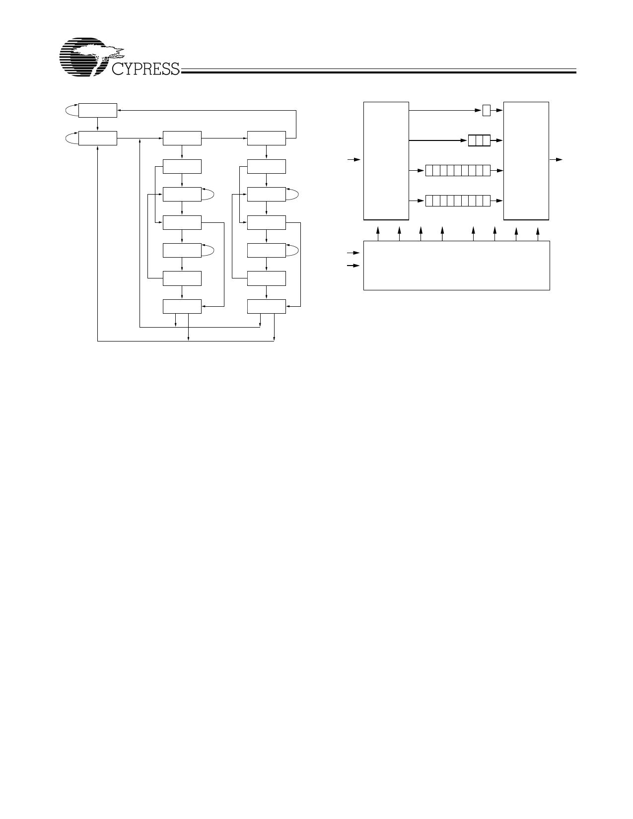
TAP Controller State Diagram
1 TEST-LOGIC
RESET
0
0 RUN-TEST/ 1
IDLE
SELECT
1
DR-SCAN
0
1
CAPTURE-DR
0
SHIFT-DR 0
1
1
EXIT1-DR
0
PAUSE-DR 0
1
0
EXIT2-DR
1
UPDATE-DR
10
SELECT
1
IR-SCAN
0
1
CAPTURE-IR
0
SHIFT-IR
0
1
1
EXIT1-IR
0
PAUSE-IR 0
1
0
EXIT2-IR
1
UPDATE-IR
10
The 0/1 next to each state represents the value of TMS at the
rising edge of TCK.
Test Access Port (TAP)
Test Clock (TCK)
The test clock is used only with the TAP controller. All inputs
are captured on the rising edge of TCK. All outputs are driven
from the falling edge of TCK.
Test Mode Select (TMS)
The TMS input is used to give commands to the TAP controller
and is sampled on the rising edge of TCK. It is allowable to
leave this ball unconnected if the TAP is not used. The ball is
pulled up internally, resulting in a logic HIGH level.
Test Data-In (TDI)
The TDI ball is used to serially input information into the
registers and can be connected to the input of any of the
registers. The register between TDI and TDO is chosen by the
instruction that is loaded into the TAP instruction register. For
information on loading the instruction register, see figure. TDI
is internally pulled up and can be unconnected if the TAP is
unused in an application. TDI is connected to the most signif-
icant bit (MSB) of any register. (See Tap Controller Block
Diagram.)
Test Data-Out (TDO)
The TDO output ball is used to serially clock data-out from the
registers. The output is active depending upon the current
state of the TAP state machine. The output changes on the
falling edge of TCK. TDO is connected to the least significant
bit (LSB) of any register. (See Tap Controller State Diagram.)
TAP Controller Block Diagram
0
Bypass Register
210
Selection
TDI
Circuitry
Instruction Register
Selection
TDO
31 30 29 . . . 2 1 0
Circuitry
Identification Register
x . . . . . 210
Boundary Scan Register
TCK
TMS
TAP CONTROLLER
Performing a TAP Reset
A RESET is performed by forcing TMS HIGH (VDD) for five
rising edges of TCK. This RESET does not affect the operation
of the SRAM and may be performed while the SRAM is
operating.
At power-up, the TAP is reset internally to ensure that TDO
comes up in a High-Z state.
TAP Registers
Registers are connected between the TDI and TDO balls and
allow data to be scanned into and out of the SRAM test
circuitry. Only one register can be selected at a time through
the instruction register. Data is serially loaded into the TDI ball
on the rising edge of TCK. Data is output on the TDO ball on
the falling edge of TCK.
Instruction Register
Three-bit instructions can be serially loaded into the instruction
register. This register is loaded when it is placed between the
TDI and TDO balls as shown in the Tap Controller Block
Diagram. Upon power-up, the instruction register is loaded
with the IDCODE instruction. It is also loaded with the IDCODE
instruction if the controller is placed in a reset state as
described in the previous section.
When the TAP controller is in the Capture-IR state, the two
least significant bits are loaded with a binary “01” pattern to
allow for fault isolation of the board-level serial test data path.
Bypass Register
To save time when serially shifting data through registers, it is
sometimes advantageous to skip certain chips. The bypass
register is a single-bit register that can be placed between the
TDI and TDO balls. This allows data to be shifted through the
SRAM with minimal delay. The bypass register is set LOW
(VSS) when the BYPASS instruction is executed.
Boundary Scan Register
The boundary scan register is connected to all the input and
bidirectional balls on the SRAM.
The boundary scan register is loaded with the contents of the
RAM I/O ring when the TAP controller is in the Capture-DR
Document #: 38-05556 Rev. *A
Page 11 of 30
Share Link: