AD7173-8(Rev0) Ver la hoja de datos (PDF) - Analog Devices
Número de pieza
componentes Descripción
Fabricante
AD7173-8
(Rev.:Rev0)
(Rev.:Rev0)
Analog Devices

AD7173-8 Datasheet PDF : 64 Pages
| |||
Data Sheet
AD7173-8
TIMING CHARACTERISTICS
IOVDD = 2 V to 5.5 V, DGND = 0 V, Input Logic 0 = 0 V, Input Logic 1 = IOVDD, CLOAD = 20 pF, unless otherwise noted.
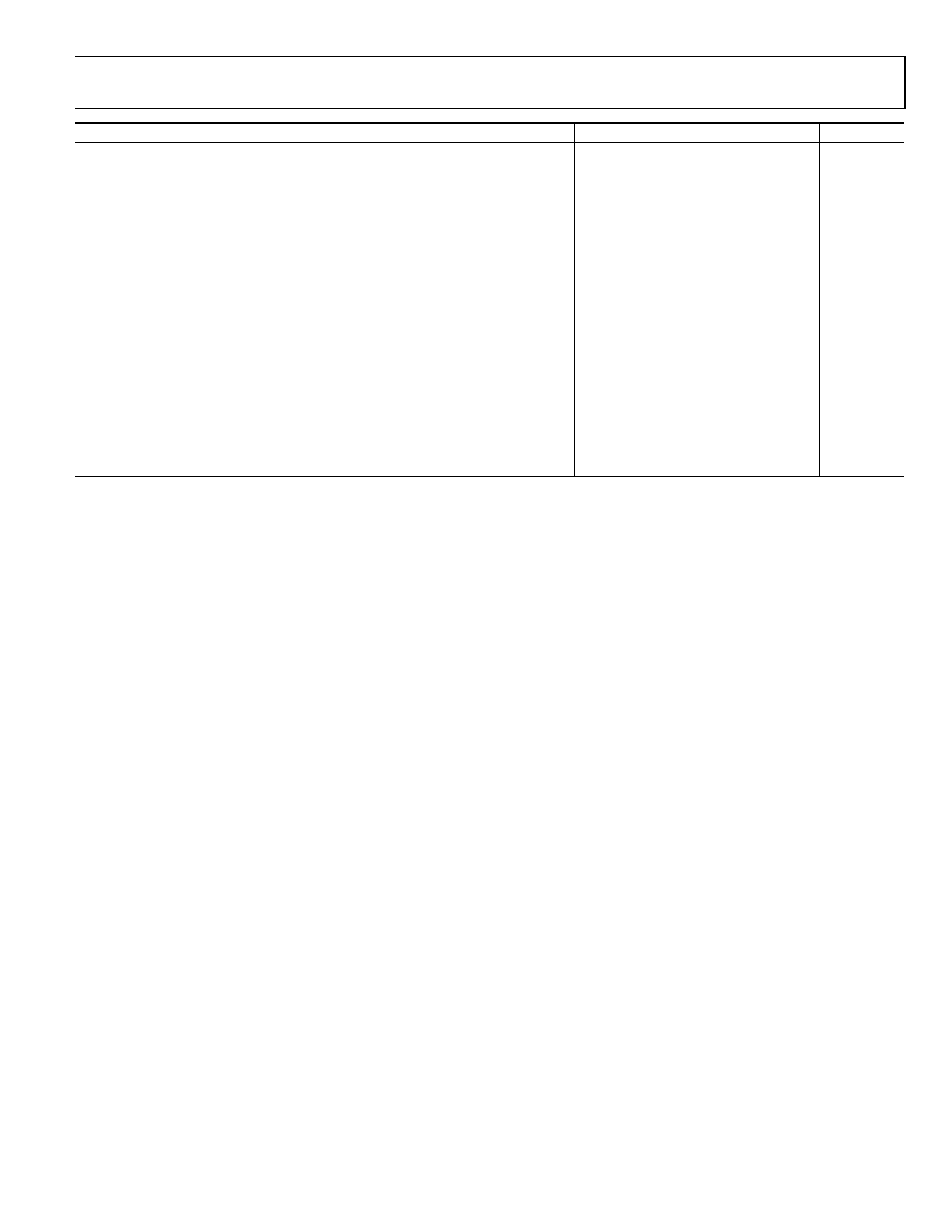
Table 2.
Parameter
SCLK PULSE WIDTH
t3
t4
READ OPERATION
t1
t2 3
t5 5
t6
t7
WRITE OPERATION
t8
t9
t10
t11
Limit at TMIN, TMAX
25
25
0
15
40
0
12
25
2.5
20
0
10
0
8
8
5
Unit
Test Conditions/Comments1, 2
ns min
ns min
SCLK high pulse width
SCLK low pulse width
ns min
ns max
ns max
ns min
ns max
ns max
ns min
ns max
ns min
ns min
CS falling edge to DOUT/RDY active time
IOVDD = 4.5 V to 5.5 V
IOVDD = 2 V to 3.6 V
SCLK active edge to data valid delay4
IOVDD = 4.5 V to 5.5 V
IOVDD = 2 V to 3.6 V
Bus relinquish time after CS inactive edge
SCLK inactive edge to CS inactive edge
SCLK inactive edge to DOUT/RDY high/low
ns min
ns min
ns min
ns min
CS falling edge to SCLK active edge setup time4
Data valid to SCLK edge setup time
Data valid to SCLK edge hold time
CS rising edge to SCLK edge hold time
1 Sample tested during initial release to ensure compliance.
2 See Figure 2 and Figure 3.
3 The time required for the output to cross the VOL or VOH limits.
4 The SCLK active edge is the falling edge of SCLK.
5 RDY returns high after a read of the data register. In single conversion mode and continuous conversion mode, the same data can be read again, if required, while RDY
is high. It is important to ensure that subsequent reads do not occur close to the next output update. If the continuous read feature is enabled, the digital word can be
read only once.
Timing Diagrams
CS (I)
DOUT/RDY (O)
SCLK (I)
t1
t2
MSB
t3
t6
t5
LSB
t7
t4
I = INPUT, O = OUTPUT
Figure 2. Read Cycle Timing Diagram
CS (I)
t8
t11
SCLK (I)
DIN (I)
t9
t10
MSB
LSB
I = INPUT, O = OUTPUT
Figure 3. Write Cycle Timing Diagram
Rev. 0 | Page 7 of 64
Share Link: