CY7C65213-28PVXI Ver la hoja de datos (PDF) - Cypress Semiconductor
Número de pieza
componentes Descripción
Fabricante
CY7C65213-28PVXI Datasheet PDF : 29 Pages
| |||
CY7C65213
CY7C65213A
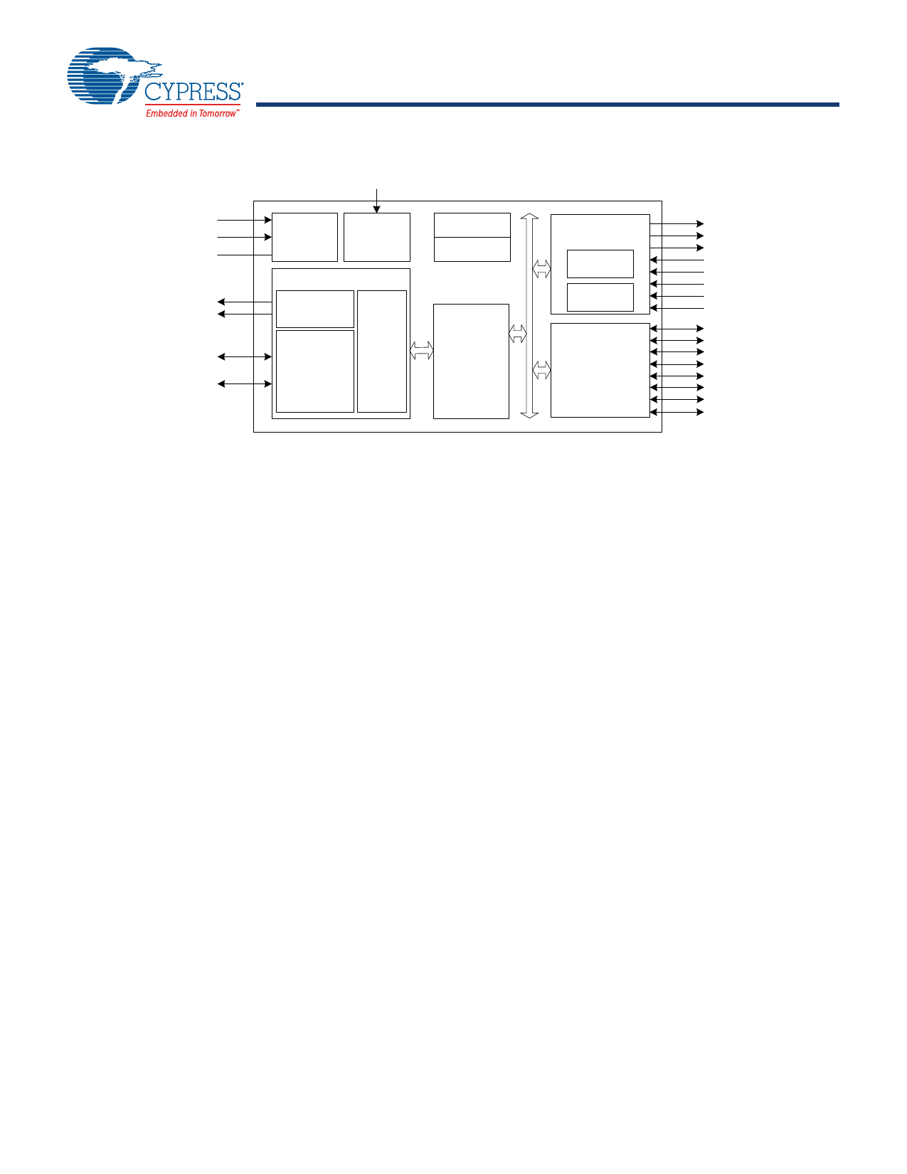
Block Diagram – CY7C65213/CY7C65213A
RESET#
VCCIO
VCC
VCCD
BCD
USBDP
USBDM
Voltage
Regulator
Reset
USB
Battery
Charger
Detection
USB
Transceiver
SIE
with
Integrated
Resistor
Internal
48 MHz OSC
Internal
32 KHz OSC
512 Bytes
Flash
Memory
UART
256 Bytes
TX Buffer
256 Bytes
RX Buffer
GPIO
TXD
DTR#
RTS#
RXD
RI#
DSR#
DCD#
CTS#
GPIO0
GPIO1
GPIO2
GPIO3
GPIO4
GPIO5
GPIO6
GPIO7
Functional Overview
CY7C65213/CY7C65213A is a fully integrated USB-to-UART
bridge that provides a simple method to upgrade UART-based
devices to USB with a minimal number of components.
CY7C65213/CY7C65213A includes a USB 2.0 Full-Speed
controller, a UART transceiver, an internal regulator, an internal
oscillator, and a 512-byte flash in a 32-pin QFN and 28-pin SSOP
package.
The internal flash is used to store custom-specific USB
descriptors and GPIO configuration. This is done in-system
using a configuration utility that communicates over the USB
interface.
Cypress provides royalty-free Virtual COM Port (VCP) device
drivers. The drivers allow the device to appear as a COM port in
PC applications. All UART signals, including handshaking and
control signals, are implemented.
USB and Charger Detect
USB
CY7C65213/CY7C65213A has a built-in USB 2.0 Full-Speed
transceiver. The transceiver incorporates an internal USB series
termination resistor on the USB data lines and a 1.5-k pull-up
resistor on the USBDP.
Charger Detection
CY7C65213/CY7C65213A supports BCD for Peripheral Detect
only and complies with the USB Battery Charging Specification,
Rev. 1.2. It supports the following charging ports:
■ Standard Downstream Port (SDP): Allows the system to draw
up to 500-mA current from the host
■ Charging Downstream Port (CDP): Allows the system to draw
up to 1.5-A current from the host
■ Dedicated Charging Port (DCP): Allows the system to draw up
to 1.5-A of current from the wall charger
Serial Communication
CY7C65213/CY7C65213A has a serial communication block
(SCB). Each SCB can implement UART interface. A 256-byte
buffer is available in both the TX and RX lines.
Document Number: 001-81011 Rev. *M
UART Interface
The UART interface provides asynchronous serial
communication with other UART devices operating at speeds of
up to 3 Mbits/second. It supports 7 to 8 data bits, 1 to 2 stop bits,
odd, even, mark, space, and no parity. The UART interface
supports full-duplex communication with a signaling format
compatible with the standard UART protocol. In CY7C65213,
UART pins may be interfaced to industry standard
RS232/RS422 transceivers whereas in CY7C65213A these
UART pins may be interfaced to RS232/RS422/RS485
transceivers.
Common UART functions, such as parity error and frame error,
are supported. A 256-byte buffer is available in both TX and RX
directions. CY7C65213/CY7C65213A supports baud rates
ranging from 300 baud to 3 Mbaud. UART baud rates can be set
using the configuration utility.
Notes:
Parity error gets detected when UART transmitter device is
configured for odd parity and UART receiver device is configured
for even parity.
Frame error gets detected when UART transmitter device is
configured for 7 bits data width and 1 stop bit, whereas UART
receiver device is configured for 8 bit data width and 2 stop bits.
UART Flow Control
The CY7C65213/CY7C65213A device supports UART
hardware flow control using control signal pairs, such as RTS#
(Request to Send) / CTS# (Clear to Send) and DTR# (Data
Terminal Ready) / DSR# (Data Set Ready).
The following sections describe the flow control signals:
■ CTS# (Input) / RTS# (Output)
CTS# can pause or resume data transmission over the UART
interface. Data transmission can be paused by de-asserting the
CTS signal and resumed by using CTS# assertion. The pause
and resume operation does not affect data integrity. With flow
control enabled, receive buffer has a watermark level of 93%.
After the data in the receive buffer reaches that level, the RTS#
signal is de-asserted, instructing the transmitting device to stop
data transmission. The start of data consumption by the
Page 4 of 29
Share Link: 