UP7706 Ver la hoja de datos (PDF) - Unspecified
Número de pieza
componentes Descripción
Fabricante
UP7706 Datasheet PDF : 12 Pages
| |||
uP7706
Application Information
The uP7706 is a high performance linear regulator
specifically designed to deliver up to 3A output current with
very low input voltage and ultra low dropout voltage. With
dual-supply configuration, the uP7706 operates with a wide
input voltage VIN range from 1.0V to 5.5V and is ideal for
applications where VOUT is very close to VIN .
Supply Voltage for Control Circuit VCNTL
Unlike other linear regulators that use a P-Channel
MOSFET as the pass transistor, the uP7706 uses an N-
Channel as the pass transistor. N-Channel MOSFET
provides lower on-resistance and better stability meeting
stringent requirements of current generation
microprocessors and other sensitive electronic devices.
The drain of N-Channel MOSFET is connected to VIN and
the source is connected to VOUT. This requires that the
supply voltage VCNTL for control circuit is at least 1.5V higher
than the output voltage to provide enough overdrive capability
for the pass transistor thus to achieve low dropout and fast
transient response. It is highly recommended to bias the
device with 5V voltage source if available.
Use a minimum 0.1uF ceramic capacitor plus a 10Ω
resistor to locally bypass the control voltage.
Input/Output Capacitor Selection
The uP7706 has a fast transient response that allows it to
handle large load changes associated with high current
applications. Proper selection of the of the output capacitor
and it’s ESR value determines stable operation and
optimizes performance. The typical application circuit
shown in Figure 1 was tested with a wide range of different
capacitors. The circuit was found to be unconditionally
stable with capacitor values from 10ìF to 2200ìF and ESR
ranging from 0.5mΩ to greater then 75mΩ.
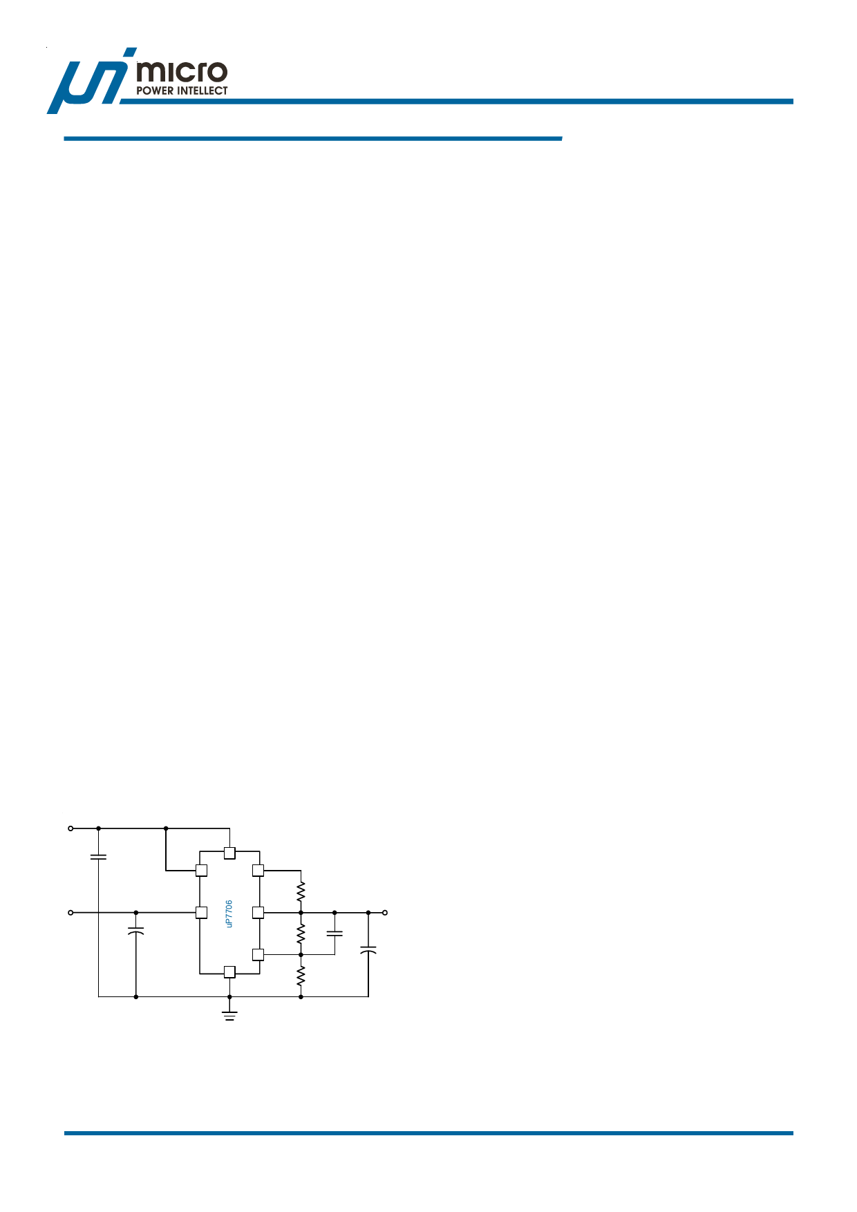
5VCC
C1
0.1uF
VIN
C2
22uF
CNTL
4
EN
2
POK
1
VIN
3
VOUT
6
FB
7
8
GND
R3
10K
R2
12.5K
R1
10K
VOUT
C4
option
C3
100uF
Figure 1. Typical Application Circuit
Input capacitor: A minimum of 10uF ceramic capacitor is
recommended to be placed directly next to the VIN pin.
This allows for the device being some distance from any
bulk capacitance on the rail. Additionally, bulk capacitance
may be added closely to the input supply pin of the uP7706
to ensure that VIN does not sag, improving load transient
response.
Output capacitor: A minimum bulk capacitance of 33uF,
along with a 0.1uF ceramic decoupling capacitor is
recommended. Increasing the bulk capacitance will improve
the overall transient response. The use of multiple lower
value ceramic capacitors in parallel to achieve the desired
bulk capacitance will not cause stability issues. Although
designed for use with ceramic output capacitors, the uP7706
is extremely tolerant of output capacitor ESR values and
thus will also work comfortably with tantalum output
capacitors.
Thermal Consideration
The uP7706 integrates internal thermal limiting function to
protect the device from damage during fault conditions.
However, continuously keeping the junction near the thermal
shutdown temperature may remain possibility to affect
device reliability. It is highly recommended to keep the
junction temperature below the recommended operation
condition 125OC for maximum reliability.
Power dissipation in the device is calculated as:
PD = (VIN - VOUT) x IOUT + VCNTL x ICNTL
It is adequate to neglect power loss with respective to
control circuit VCNTL x ICNTL when considering thermal
management in uP7706 Take the following moderate
operation condition as an example: VIN = 2.5V, VOUT = 1.5V,
IOUT = 2A, the power dissipation is:
PD = (1.8V- 1.2V) x 2A = 2.0W
This power dissipation is conducted through the package
into the ambient environment, and, in the process, the
temperature of the die (TJ) rises above ambient. Large power
dissipation may cause considerable temperature raise in
the regulator in large dropout applications. The geometry
of the package and of the printed circuit board (PCB) greatly
influence how quickly the heat is transferred to the PCB
and away from the chip. The most commonly used thermal
metrics for IC packages are thermal resistance from the
chip junction to the ambient air surrounding the package
(θJA):
θJA = ( TJ -TA ) / PD
θJA specified in the Thermal Information section is measured
in the natural convection at TA = 25OC on a high effective
thermal conductivity test board (4 Layers, 2S2P) of JEDEC
51-7 thermal measurement standard. The case point of
uPI Semiconductor Corp., http://www.upi-semi.com
9
Rev. F00, File Name: uP7706-DS-F0000
Share Link: 