UP7706 Ver la hoja de datos (PDF) - Unspecified
Número de pieza
componentes Descripción
Fabricante
UP7706 Datasheet PDF : 12 Pages
| |||
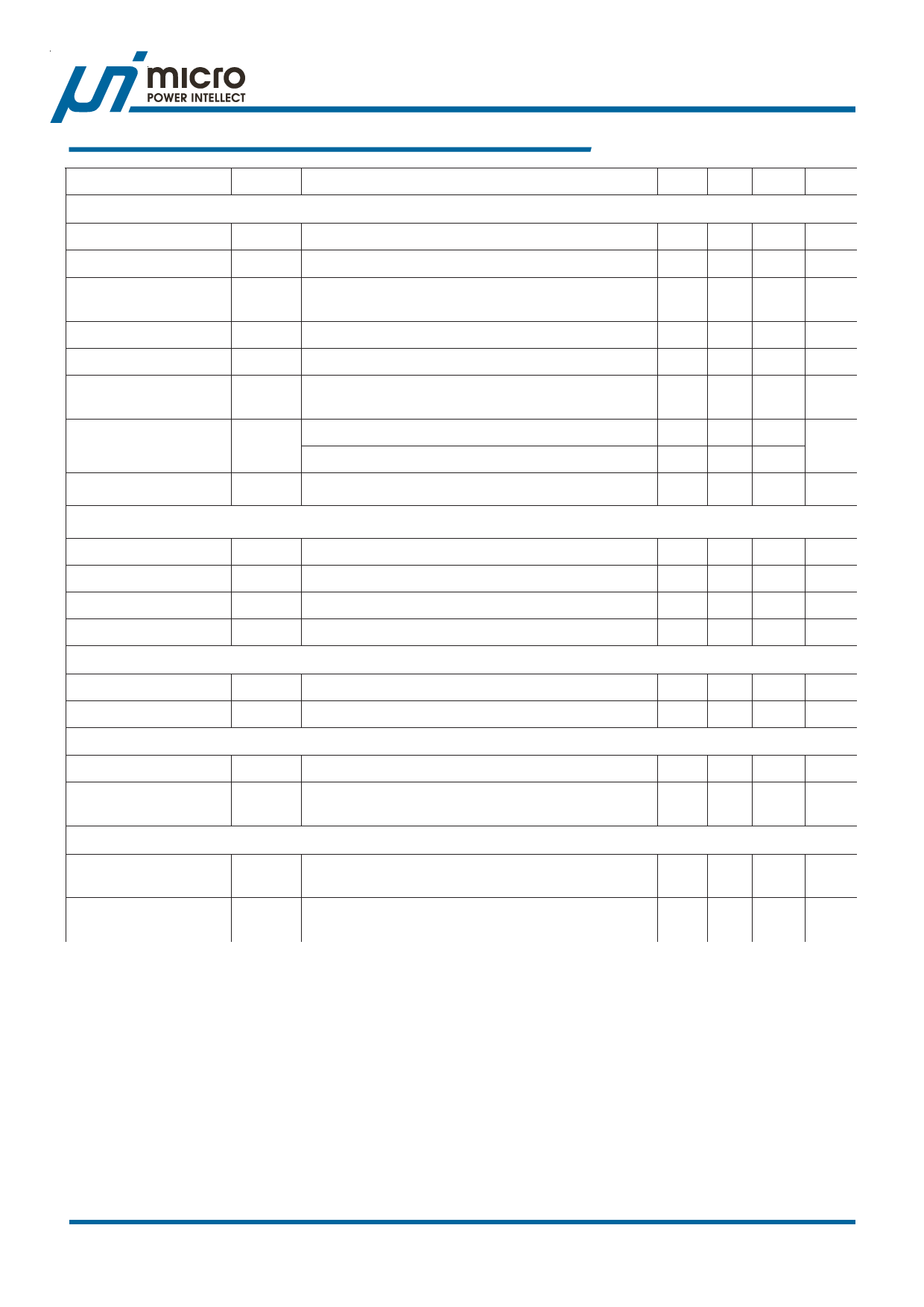
uP7706
Electrical Characteristics
Parameter
Symbol
Test Conditions
Feedback Voltage
Reference Voltage
Feedback Input Current
VIN Line Regulation
VCNTL Line Regulation
Load Regulation
Load Regulation over
Temperature
Dropout Voltage
VOUT Pull Low Resistance
VREF
VCNTL = VIN = VEN = 5.0V, IOUT = 0A. VOUT = VREF
IFB
VREF(LINE)
1.2V < VIN < 5.0V, VCNTL = VEN = 5.0V, IOUT = 0A. VOUT =
VREF
VREF(CNTL) VIN = 3.3V, IOUT = 0A. VOUT = VREF
VREF(LOAD) 10mA < IOUT < 3A, VCNTL = VIN = VEN = 5.0V, VOUT = VREF
VREF(LOAD)
10mA < IOUT < 3A, VCNTL = VIN = VEN = 5.0V, VOUT = VREF,
-40OC < TJ < 125OC
VDROP
IOUT = 2A, VCNTL = VEN = 5.0V, VOUT = VREF
I OUT = 3A, VCNTL = VEN = 5.0V, VOUT = VREF
VCNTL = VIN = 5.0V, VEN = 0V,
Enable
Enable High Level
VEN
Disable Low Level
VSD
EN Input Current
IEN
EN Input Impedance
ZEN
PWROK
VEN = VCNTL = 5.0V
FB Power OK Threshold
Power OK Hysteresis
Overcurrent Protection
VPOKTH
VPOKHYS
IOUT = 0A, VCNTL = VIN = VEN = 5.0V, VOUT = VREF
IOUT = 0A, VCNTL = VIN = VEN = 5.0V, VOUT = VREF
OCP Threshold Level
IOCP
Output Short Circuit
Current
ISC
Thermal Protection
VCNTL = VIN = VEN = 5.0V, VOUT = VREF
VCNTL = VIN = VEN = 5.0V, VOUT = VREF
Thermal Shutdown
Temperature
Thermal Shutdown
Hysteresis
TSD
TSDHYS
IOUT = 0A, VCNTL = VIN = VEN = 5.0V, VOUT = VREF
IOUT = 0A, VCNTL = VIN = VEN = 5.0V, VOUT = VREF
Min Typ Max Units
0.788 0.8 0.812 V
--
20
--
nA
-- 0.01 0.1 %/V
-- 0.01 0.1 %/V
-- 0.8 1.5 %/A
--
1.4
3
%
-- 200 240
mV
300 360
--
90
--
Ω
--
--
1.4
V
0.8 --
--
V
--
12 20
uA
--
65
--
KΩ
--
92
--
%
--
8
--
%
--
4
--
A
-- 100 --
mA
-- 170 --
OC
--
30
--
OC
Note 1. Stresses listed as the above “Absolute Maximum Ratings” may cause permanent damage to the device.
These are for stress ratings. Functional operation of the device at these or any other conditions beyond those
indicated in the operational sections of the specifications is not implied. Exposure to absolute maximum
rating conditions for extended periods may remain possibility to affect device reliability.
Note 2. Devices are ESD sensitive. Handling precaution recommended.
Note 3. θJA is measured in the natural convection at TA = 25°C on a low effective thermal conductivity test board of
JEDEC 51-3 thermal measurement standard.
Note 4. The device is not guaranteed to function outside its operating conditions.
uPI Semiconductor Corp., http://www.upi-semi.com
5
Rev. F00, File Name: uP7706-DS-F0000
Share Link: 