UP7706 Ver la hoja de datos (PDF) - Unspecified
Número de pieza
componentes Descripción
Fabricante
UP7706 Datasheet PDF : 12 Pages
| |||
uP7706
Functional Description
Definitions
Some important terminologies for LDO are specified below.
Dropout Voltage
The input/output voltage differential at which the regulator
output no longer maintains regulation against further
reductions in input voltage. Measured when the output drops
2% below its nominal value. Dropout voltage is affected by
junction temperature, load current and minimum input
supply requirements.
Line Regulation
The change in output voltage for a change in input voltage.
The measurement is made under conditions of low
dissipation or by using pulse techniques such that average
chip temperature is not significantly affected.
Load Regulation
The change in output voltage for a change in load current
at constant chip temperature. The measurement is made
under conditions of low dissipation or by using pulse
techniques such that average chip temperature is not
significantly affected.
Maximum Power Dissipation
The maximum total device dissipation for which the
regulator will operate within specifications.
Initialization
The uP7706 automatically initiates upon the receipt of
supply voltage and power voltage. A power on reset circuit
continuously monitors VIN and CNTL pins voltages with
rising threshold levels of 1.0V and 2.7V respectively.
Chip Enable and Soft Start
It’s recommended to maintain 50-100uA through the output
divider network for a tight load and line regulation. The
internal voltage reference is VREF = 0.8V with 1.5%
accuracy over full temperature range. This commands the
use of 0.5% or better accuracy resistors to build a precision
power supply.
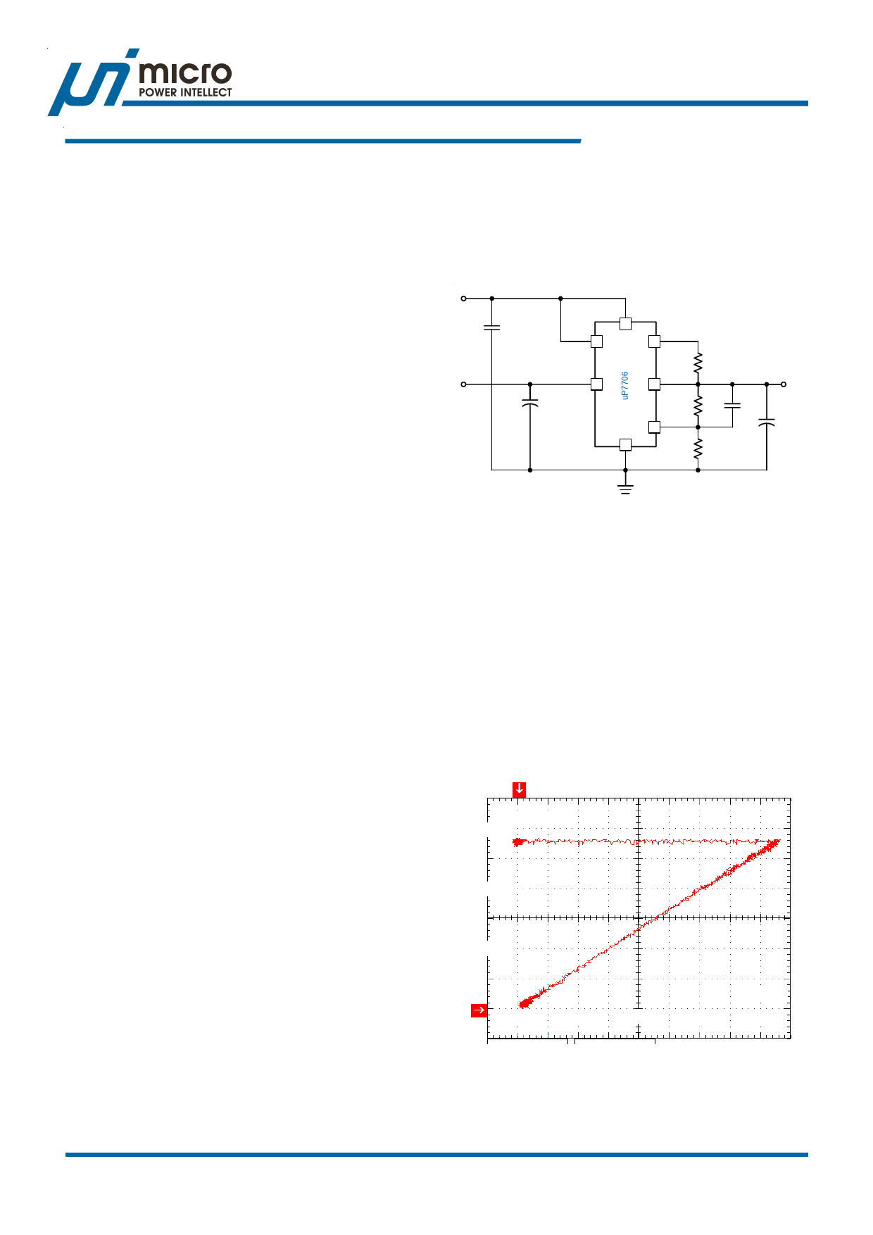
5VCC
C1
0.1uF
VIN
C2
22uF
CNTL
4
EN
2
POK
1
VIN
3
VOUT
6
FB
7
8
GND
R3
10K
R2
12.5K
R1
10K
VOUT
C4
option
C3
100uF
Figure 1. Typical application of 2.5V to 1.8V conversion
with a 5.0V control supply
Over Current Protection
The uP7706 features a foldback over current protection
function as shown in Figure 2. The current limit threshold
level is proportional to VOUT/VNOM and is typically 4A when
VOUT = VNOM, where VNOM is the target output voltage. If the
output continuously demands more current than the
maximum current, output voltage will eventually drops below
its nominal value. This, in turns, will lower its OCP threshold
level. This will limit power dissipation in the device when
over current limit happens. The power dissipation is near
zero when the output is short circuited to ground.
The uP7706 features an enable pin for enable/disable
control of the chip. Pulling VEN lower than 0.8V disables
the chip and reduces its quiescent current down to 1uA.
When disabled, an internal MOSFET of 90Ω RDS(ON) turns
on to pull output voltage to ground. Pulling VEN higher than
2.0V enables the output voltage, providing POR is
recognized. The uP7706 features soft start function that
limits inrush current for charging the output capacitors. The
soft start time is typically 2.5ms.
Output Voltage Programming
Figure 1 shows a typical application of 2.5V to 1.8V
conversion with a 5.0V control supply. The output voltage
is sensed through a voltage divider and regulated to internal
reference voltage VREF. The output voltage is programmed
as:
VOUT = VREF x (R1+R2) / R1 = 0.8V x (22.5k/10k) = 1.8V
3V VOUT
2A
1V
IOUT
0A
1A
2A
3A
4A
Figure 2. Current Limit Behavior
uPI Semiconductor Corp., http://www.upi-semi.com
3
Rev. F00, File Name: uP7706-DS-F0000
Share Link: 