UP7706 Ver la hoja de datos (PDF) - Unspecified
Número de pieza
componentes Descripción
Fabricante
UP7706 Datasheet PDF : 12 Pages
| |||
uP7706
Functional Pin Description
Pin No.
1
2
3
4
5
6
7
8
Exposed
Pad
Name Pin Function
POK
Power OK Indication. This pin is an open-drain output and is set high impedance once VOUT
reaches 92% of its rating voltage.
EN
Enable Input. Pulling this pin below 0.8V turns the regulator off, reducing the quiescent current
to a fraction of its operating value.
Input Voltage. This is the drain input to the power device that supply current to the output pin.
VIN
Large bulk capacitors with low ESR should be placed physically close to this pin o prevent the
input rail from dropping during large load transient. A 10uF ceramic capacitor is recommended
at this pin.
CNTL
NC
Supply Input for Control Circuit. This pin provides bias voltage to the control circuitry and
driver for the pass transistor.The driving capability of output current is proportioned to the VCNTL.
For the device to regulate, the voltage on this pin must be at least 1.5V greater than the output
voltage, and no less than VCNTL_MIN.
Not Internally Connected.
Output Voltage. This pin is power output of the device. A pull low resistance exists when the
VOUT
device is disabled by pulling low the EN pin. To maintain adequate transient response to large
load change, typical value of 1000uF Al electrolytic capacitor with 10uF ceramic capacitors are
recommended to reduce the effects of current transients on VOUT.
FB
GND
Feedback Voltage. This pin is the inverting input to the error amplifier. A resistor divider from
the output to GND is used to set the regulation voltage as VOUT = 0.8x(R1+R2)/R1 (V)
Ground.
GND
Ground. The exposed pad acts the dominant power dissipation path and should be soldered
to well design PCB pads as described in the Application Informations Chapter.
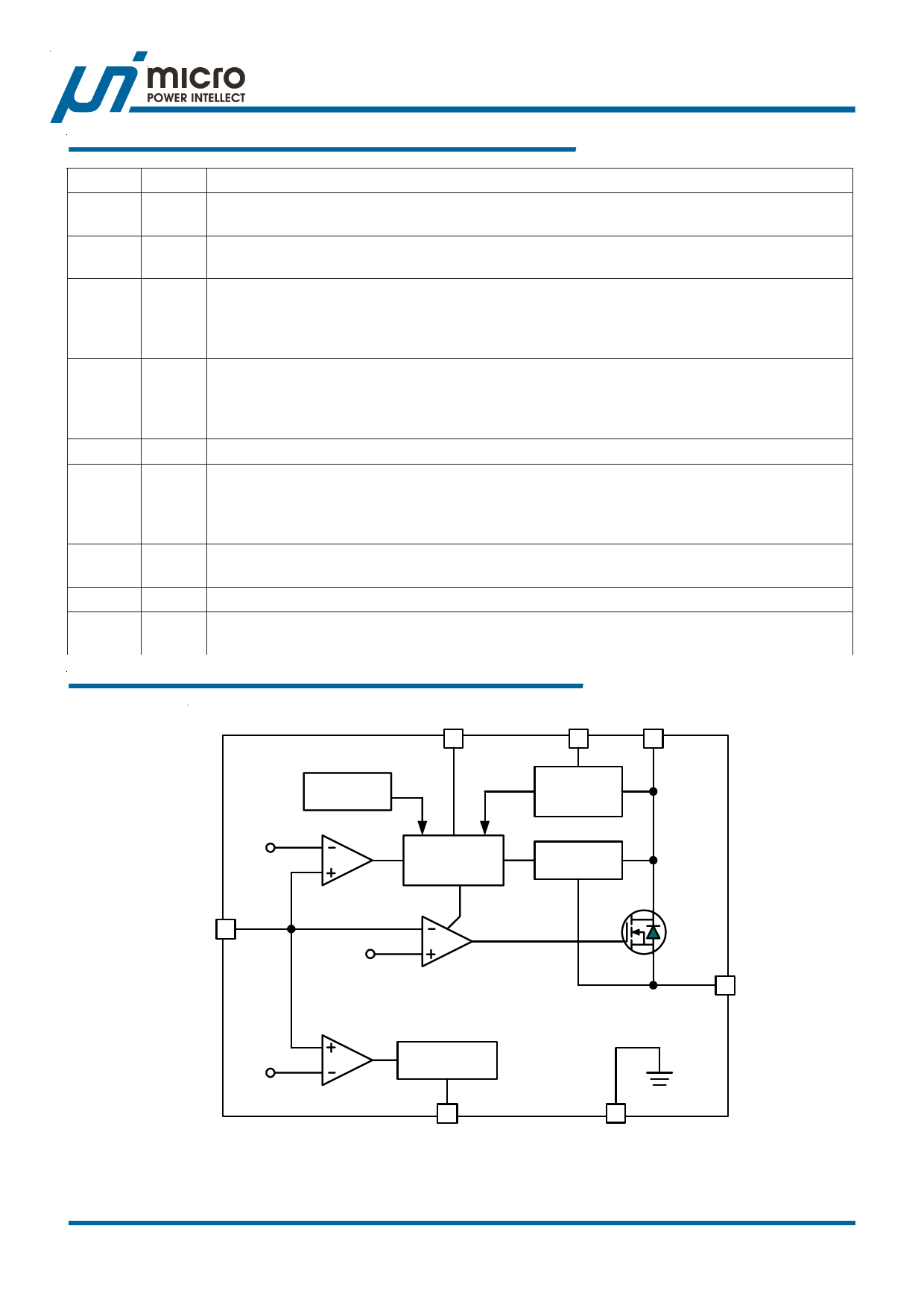
Functional Block Diagram
EN
CNTL
VIN
2
4
3
Thermal Limit
0.3V
Softstart &
Control Logic
Power On
Reset
Current Limit
FB 7
0.8V VREF
6
92% VREF
Delay
1
POK
8
GND
uPI Semiconductor Corp., http://www.upi-semi.com
2
Rev. F00, File Name: uP7706-DS-F0000
Share Link: 