UP7706 Ver la hoja de datos (PDF) - Unspecified
Número de pieza
componentes Descripción
Fabricante
UP7706 Datasheet PDF : 12 Pages
| |||
uP7706
Application Information
θJC is on the exposed pad for PSOP-8 package.
Given power dissipation PD, ambient temperature and
thermal resistance θJA, the junction temperature is
calculated as:
TJ = TA + ∆TJA = TA + PD x θJA
To limit the junction temperature within its maximum rating,
the allowable maximum power dissipation is calculated
as:
PD(MAX) = ( TJ(MAX) -TA ) /θJA
where TJ(MAX) is the maximum operation junction
temperature 125OC, TA is the ambient temperature and the
θJA is the junction to ambient thermal resistance. θJA of
PSOP-8 packages is 75OC/W on JEDEC 51-7 (4 layers,
2S2P) thermal test board with minimum copper area. The
maximum power dissipation at TA = 25¢XC can be calculated
as:
PD(MAX) = (125OC - 25OC) / 75OC/W = 1.33W
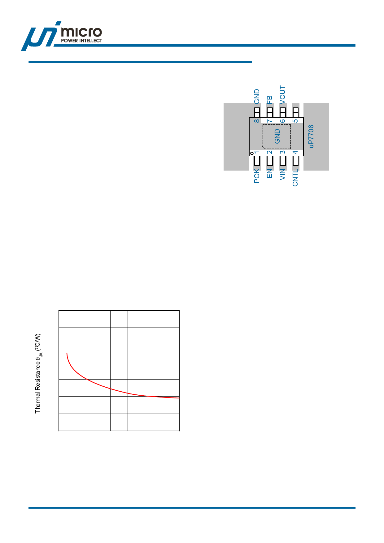
The thermal resistance θJA highly depends on the PCB
design. Copper plane under the exposed pad is an effective
heatsink and is useful for improving thermal conductivity.
Figure 3 show the relationship between thermal resistance
θJA vs. copper area on a standard JEDEC 51-7 (4 layers,
2S2P) thermal test board at TA = 25OC. A 50mm2 copper
plane reduces θJA from 75OC/W to 50OC/W and increases
maximum power dissipation from 1.33W to 2W.
Figure 4. Recommended PCB Layout.
Layout Consideration
1. Place a local bypass capacitor as closed as possible
to the VIN pin. Use short and wide traces to minimize
parasitic resistance and inductance.
2. The exposed pad should be soldered on GND plane
with maximum area and with multiple vias to inner layer
of ground place for improved thermal performance.
3. Connect voltage divider directly to the point where
regulation is required. Place voltage divider close to
the device.
100
90
80
70
60
50
40
30
0 10
20 30 40 50 60 70
Copper Area (mm2)
Figure 3. Thermal Resistance èJA vs. Copper Area
Figure 4 illustrated the recommended PCB layout for best
thermal performance.
uPI Semiconductor Corp., http://www.upi-semi.com
10
Rev. F00, File Name: uP7706-DS-F0000
Share Link: 