OX12PCI840-PQC60-A Ver la hoja de datos (PDF) - Oxford Semiconductor
Número de pieza
componentes Descripción
Fabricante
OX12PCI840-PQC60-A Datasheet PDF : 33 Pages
| |||
OXFORD SEMICONDUCTOR LTD.
OX12PCI840
4.3 Accessing logical functions
Access to the parallel port is achieved via standard I/O and memory mapping, at addresses defined by the Base Address
Registers (BARs) in configuration space. The BARs are configured by the system to allocate blocks of I/O and memory space to
the logical function, according to the size required by the function. The addresses allocated can then be used to access the
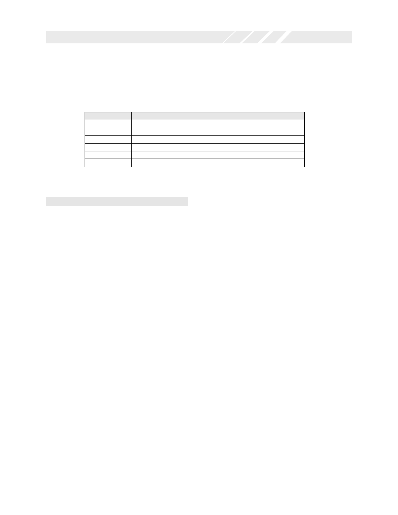
function. The mapping of these BARs is shown in Table 4.
BAR
Mapping
0
Parallel port base registers (I/O mapped)
1
Parallel port extended registers (I/O mapped)
2
Local configuration registers (I/O mapped
3
Local configuration registers (memory mapped)
4
Unused
5
Unused
Table 4: Base Address Register definition
4.3.1 PCI access to parallel port
Access to the port works with two I/O BARs corresponding
to the two sets of registers defined to operate an IEEE1284
ECP/EPP and bi-directional Parallel Port.
The user can change the I/O space block size of BAR0 or
BAR by over-writing the default values using the serial
EEPROM (see section 4.4).
Legacy parallel ports expect the upper register set to be
mapped 0x400 above the base block, therefore if the BARs
are fixed with this relationship, generic parallel port drivers
can be used to operate the device in all modes.
Example: BAR0 = 0x00000379 (8 bytes at address 0x378)
BAR1 = 0x00000779 (8 bytes at address 0x778)
If this relationship is not used, custom drivers will be
needed.
DS-0021 Jun 05
Page 11
Share Link: 