LTC1261C Ver la hoja de datos (PDF) - Linear Technology
Número de pieza
componentes Descripción
Fabricante
LTC1261C Datasheet PDF : 18 Pages
| |||
APPLICATIONS INFORMATION
VCC
LTC1261
CLK
550kHz
S
Q
R
S1
S5
C1+
C1 S4
S2
C1–
C2+
C2 S6
C2–
S3
S7
COMP 1
60mV
VREF = 1.24V
1.18V
VOUT
+
COMP 2
–
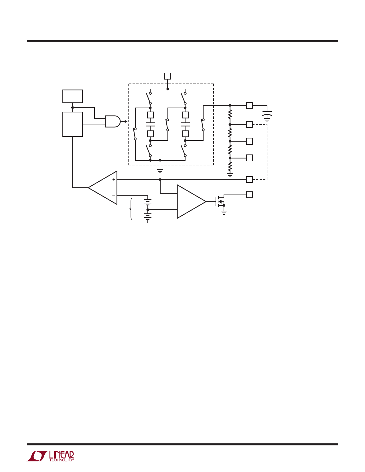
Figure 2. Block Diagram
OUT
+
124k RADJ*
COUT
226k R1*
100k R0*
50k
ADJ/COMP
REG
INTERNALLY
CONNECTED FOR
FIXED OUTPUT
VOLTAGE PARTS
LTC1261 • F02
*LTC1261CS14 ONLY
The output voltage is monitored by COMP1 which compares
a divided replica of the output at ADJ (COMP for fixed
output parts) to the internal reference. At the beginning
of a cycle the clock is low, forcing the output of the AND
gate low and charging the flying capacitors. The next rising
clock edge sets the RS latch, setting the charge pump to
transfer charge from the flying capacitors to the output
capacitor. As long as the output is below the set point,
COMP1 stays low, the latch stays set and the charge pump
runs at the full 50% duty cycle of the clock gated through
the AND gate. As the output approaches the set voltage,
COMP1 will trip whenever the divided signal exceeds the
internal 1.24V reference relative to OUT. This resets the
RS latch and truncates the clock pulses, reducing the
amount of charge transferred to the output capacitor and
regulating the output voltage. If the output exceeds the
set point, COMP1 stays high, inhibiting the RS latch and
disabling the charge pump.
COMP2 also monitors the divided signal at ADJ but it is
connected to a 1.18V reference, 5% below the main refer-
ence voltage. When the divided output exceeds this lower
reference voltage indicating that the output is within 5%
of the set value, COMP2 goes high turning on the REG
output transistor. This is an open drain N-channel device
capable of sinking 5mA with a 3.3V VCC and 8mA with
a 5V VCC. When in the “off” state (divided output more
than 5% below VREF) the drain can be pulled above VCC
without damage up to a maximum of 12V above ground.
Note that the REG output only indicates if the magnitude of
the output is below the magnitude of the set point by 5%
(i.e., VOUT > –4.75V for a –5V set point). If the magnitude
of the output is forced higher than the magnitude of the
set point ( i.e., to – 6V when the output is set for –5V) the
REG output will stay low.
For more information www.linear.com/LTC1261
1261fb
7
Share Link: 